In order to control the impedance of the PCB well, we must first understand the structure of the PCB:
Usually what we call a multilayer board is formed by laminating a core board and a prepreg. The core board is a hard, specific thickness, two-bread copper plate, which is the basic material of the printed board. . The prepreg constitutes the so-called wetting layer, which plays the role of bonding the core board. Although it also has a certain initial thickness, its thickness will change during the pressing process.
Usually the two outermost dielectric layers of the multilayer board are both wetting layers, and a separate copper foil layer is used as the outer copper foil on the outside of the two layers. The original thickness specifications of the outer copper foil and inner copper foil are generally 0.5OZ, 1OZ, 2OZ (1OZ is about 35um or 1.4mil), but after a series of surface treatments, the final thickness of the outer copper foil is average It will increase by about 1OZ. The inner copper foil is the copper clad on both sides of the core board, and its final thickness is very small from the original thickness, but due to etching, it is generally reduced by a few um.
The outermost layer of the multilayer board is the solder mask, which is what we often call "green oil". Of course, it can also be yellow or other colors. The thickness of the solder mask is generally not easy to accurately determine. The area without copper foil on the surface is slightly thicker than the area with copper foil. However, because of the lack of copper foil thickness, the copper foil still appears more prominent. When we use You can feel it when your finger touches the surface of the printed board.
When making a printed board with a certain thickness, on the one hand, it is required to select the parameters of various materials reasonably. On the other hand, the final forming thickness of the prepreg will be smaller than the initial thickness. The following is a typical 6-layer laminate structure:
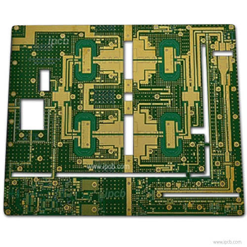
Sixteen-layer circuit board structure, six-layer impedance circuit board laminated structure diagram, this is a design laminated structure of a 16-layer blind buried via circuit board.
PCB parameters:
Different circuit board manufacturers have slight differences in PCB parameters:

Surface copper foil:
There are three types of surface copper foil material thicknesses that can be used: 12um, 18um and 35um. The final thickness after processing is about 44um, 50um and 67um.
Core board: Our commonly used board is S1141A, standard FR-4, two copper breads, and the available specifications can be determined by contacting the manufacturer.
prepreg:
specifications (original thickness) are 7628 (0.185mm), 2116 (0.105mm), 1080 (0.075mm), 3313 (0.095mm), the thickness after the actual pressing is usually about 10-15um smaller than the original value. Up to 3 prepregs can be used for the same wetting layer, and the thickness of the 3 prepregs cannot be the same. At least one prepreg can be used, but some manufacturers require at least two. If the thickness of the prepreg is not enough, the copper foils on both sides of the core board can be etched away, and then the prepregs can be used for adhesion on both sides, so that a thicker wetting layer can be achieved.
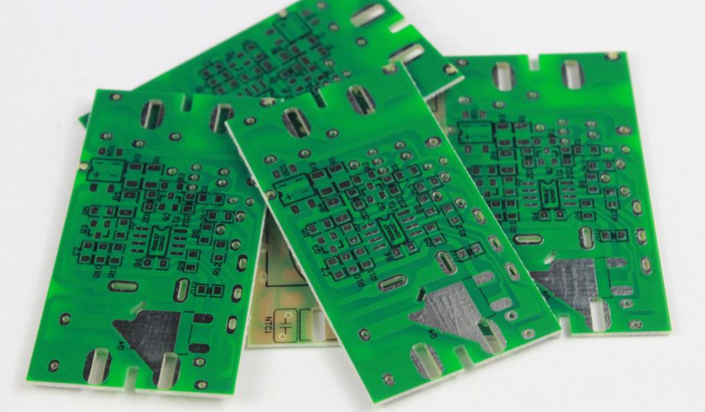
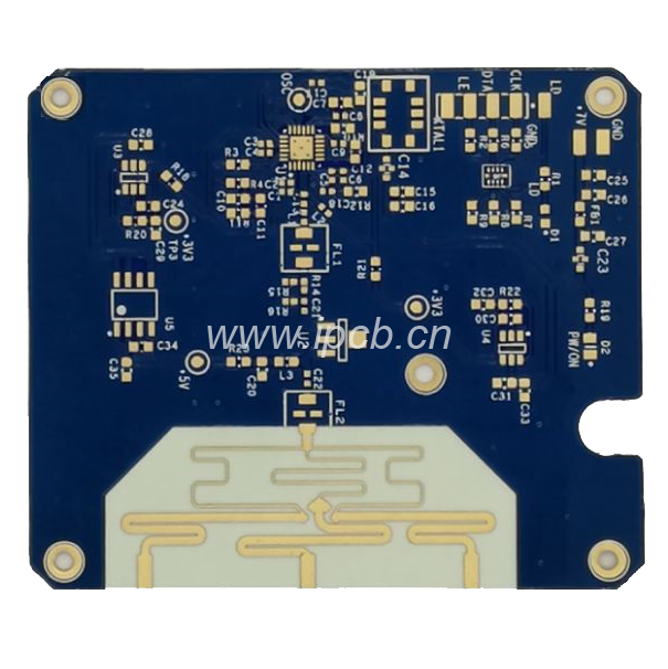
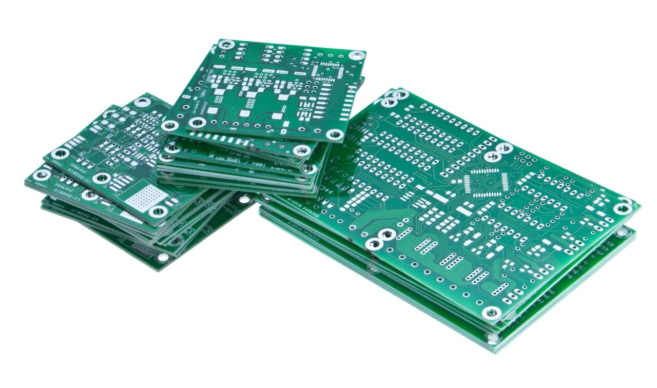
The company has a professional circuit board production team, with more than 110 senior engineers and professional management personnel with more than 15 years of work experience; it has domestic leading automated production equipment, PCB products include 1-32 layer boards, high TG boards, and thick copper boards, Rigid and flexible boards, high frequency boards, mixed dielectric laminates, blind buried vias, metal substrates and halogen-free boards.
Fast samples of high-precision circuit boards, 6-7 days for bulk orders for single and double panels, 9-12 days for 4-8 layers, 15-20 days for 10-16 layers, and 20 days for HDI boards. Double-sided proofing can be delivered in as fast as 8 hours.