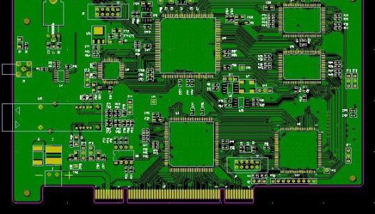
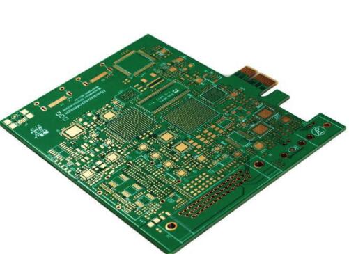
The interconnect of printed circuit board system includes chip-to-circuit board, interconnect within PCB and interconnect between PCB and external devices. In RF design, the electromagnetic characteristics at the interconnect point is one of the main problems faced by engineering design. This paper introduces various techniques of the above three types of interconnect design, including device installation methods, isolation of wiring and measures to reduce lead inductance.
There are signs that printed circuit boards are being designed with increasing frequency. As data rates continue to increase, the bandwidth required for data transmission also pushes the signal frequency ceiling to 1GHz or higher. This high frequency signal technology, although far beyond the millimeter wave technology (30GHz), does involve RF and low-end microwave technology.

RF engineering design methods must be able to handle the stronger electromagnetic field effects that are typically generated at higher frequencies. These electromagnetic fields can induce signals on adjacent signal lines or PCB lines, causing undesirable crosstalk (interference and total noise) and harming system performance. Backloss is mainly caused by impedance mismatch, which has the same effect on the signal as additive noise and interference.
High return loss has two negative effects: 1. The signal reflected back to the signal source will increase the noise of the system, making it more difficult for the receiver to distinguish noise from signal; 2. 2. Any reflected signal will essentially degrade the quality of the signal because the shape of the input signal changes.
Although digital systems are very fault tolerant because they only deal with 1 and 0 signals, the harmonics generated when the pulse is rising at high speed cause the signal to be weaker at higher frequencies. Although forward error correction can eliminate some of the negative effects, part of the system bandwidth is used to transmit redundant data, resulting in performance degradation. A better solution is to have RF effects that help rather than detract from signal integrity. The total return loss at the frequency of the digital system (usually the poorer data points) is -25dB, equivalent to a VSWR of 1.1.
PCB design aims to be smaller, faster and less costly. For RFPCB, high-speed signals sometimes limit the miniaturization of PCB designs. At present, the main method to solve the crosseration problem is to carry out ground connection management, conduct spacing between wiring and reduce lead inductance. The main method to reduce the return loss is impedance matching. This method includes effective management of insulation materials and isolation of active signal lines and ground lines, especially between the state of the signal line and ground.
Because interconnect is the weak link in the circuit chain, in RF design, the electromagnetic properties of interconnect point is the main problem facing engineering design, each interconnect point should be investigated and the existing problems solved. Circuit board in the connection includes chip-to-circuit board interconnection, PCB interconnection and signal input/output interconnection between PCB and external devices.