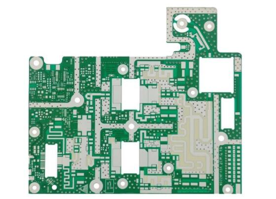
With the development of the electronics industry, the integration level of electronic components is getting higher and higher, and the volume is getting smaller and smaller, and BGA type packaging is generally used. Therefore, the circuits of multi-layer PCB will become smaller and smaller, and the number of layers will increase. To reduce the line width and line spacing is to use the limited area as much as possible, and to increase the number of layers is to use space. The main line of the future circuit board will be 2-3mil, or smaller.
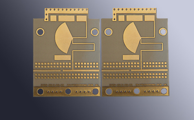
Dingji has a professional circuit board production team, with more than 110 senior engineers and professional management personnel with more than 15 years of work experience; it has domestic leading automatic production equipment, PCB products include 1-32 layer boards, high TG boards, thick Copper board, rigid-flex board, high frequency board, mixed dielectric laminate, blind buried via board, metal substrate and halogen-free board.
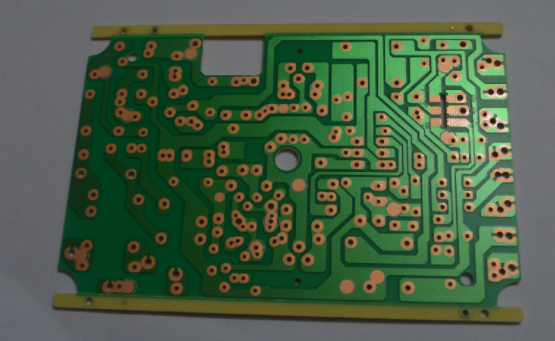
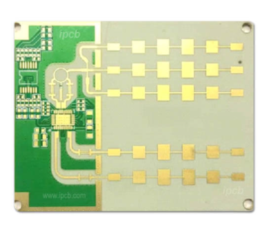
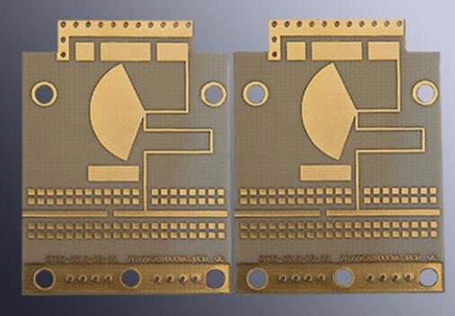
Via is one of the important components of multilayer PCB. The cost of drilling usually accounts for 30% to 40% of the cost of multilayer PCB manufacturing. Simply put, every hole on the PCB can be called a via.

From the perspective of function, vias can be divided into two categories: one is used for electrical connection between layers; the other is used for fixing or positioning devices. In terms of process, these vias are generally divided into three categories, namely blind vias, buried vias and through vias. Blind vias are located on the top and bottom surfaces of the printed circuit board and have a certain depth. They are used to connect the surface line and the underlying inner line. The depth of the hole usually does not exceed a certain ratio (aperture). Buried hole refers to the connection hole located in the inner layer of the printed circuit board, which does not extend to the surface of the circuit board.
Fast samples of high-precision circuit boards, 6-7 days for bulk orders for single and double panels, 9-12 days for 4-8 layers, 15-20 days for 10-16 layers, and 20 days for HDI boards. Double-sided proofing can be delivered in as fast as 8 hours.
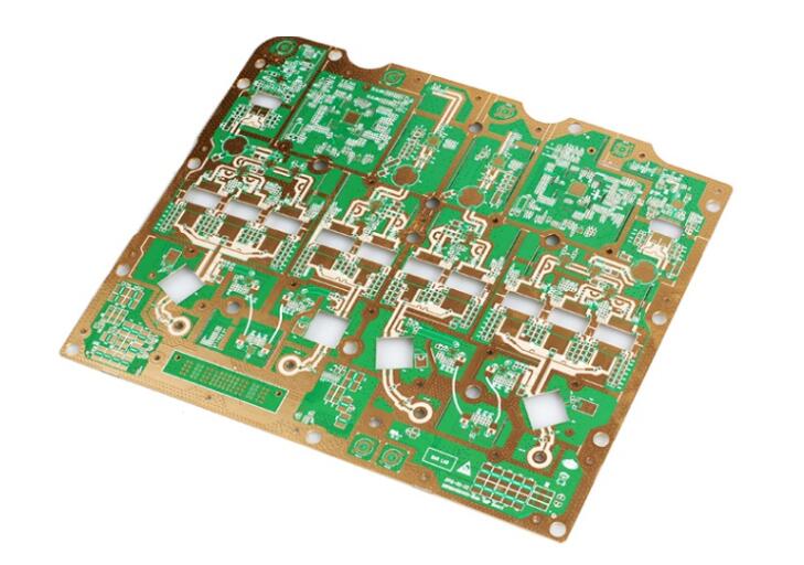
Difficult multi-layer PCB circuit board processing manufacturer-dingji electronics
Back to list source: Dingji Electronics PCB Release Date 2019-09-18 Views: 273
With the development of the electronics industry, the integration level of electronic components is getting higher and higher, and the volume is getting smaller and smaller, and BGA type packaging is generally used. Therefore, the circuits of multi-layer PCB will become smaller and smaller, and the number of layers will increase. To reduce the line width and line spacing is to use the limited area as much as possible, and to increase the number of layers is to use space. The main line of the future circuit board will be 2-3mil, or smaller.
Dingji has a professional circuit board production team, with more than 110 senior engineers and professional management personnel with more than 15 years of work experience; it has domestic leading automatic production equipment, PCB products include 1-32 layer boards, high TG boards, thick Copper board, rigid-flex board, high frequency board, mixed dielectric laminate, blind buried via board, metal substrate and halogen-free board.
Via is one of the important components of multilayer PCB. The cost of drilling usually accounts for 30% to 40% of the cost of multilayer PCB manufacturing. Simply put, every hole on the PCB can be called a via.
iPCB specializes in the production of thick copper circuit boards, thick copper circuit boards, precision double-sided circuit boards, impedance PCB circuit boards, blind hole circuit boards, flexible circuit boards, buried hole circuit boards, blind buried holes circuit boards, mobile phone circuit boards, Bluetooth circuits Board, car circuit board, transportation circuit board, security circuit board, HDI circuit board, aerospace spectrograph circuit board, industrial control PCB circuit board, communication PCB circuit board, smart home PCB circuit board, military PCB circuit board, medical PCB circuit High-precision, high-difficulty, thick copper circuit boards, such as high-precision, high-difficulty, production types: HDI mobile phone circuit boards, high-frequency circuit boards, radio frequency circuit boards, impedance circuit boards, thick copper circuit boards (12OZ), soft and hard bonding boards, Yin-Yang copper boards, Aluminum substrates, mixed pressure boards, backplanes, buried capacitance and buried resistance boards, HDI circuit boards produced by the company, precision double-sided multilayer circuit boards, flexible circuit boards, impedance circuit boards, flexible circuit boards, and blind buried vias The certificates required for the production of circuit boards, such as UL, SGS, ISO9001, RoHS, QS9000, TS16949, are used in a wide range of products, such as computers, medical facilities, vehicles, various communication devices, military, aerospace, etc.