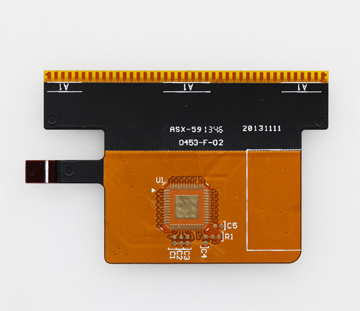
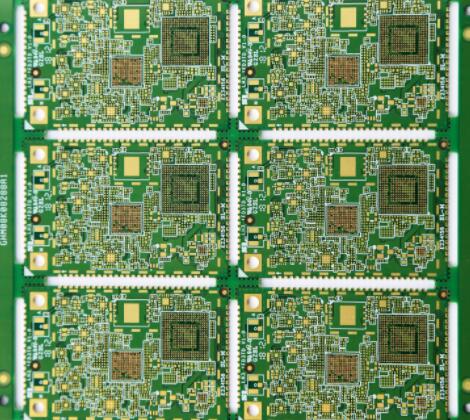
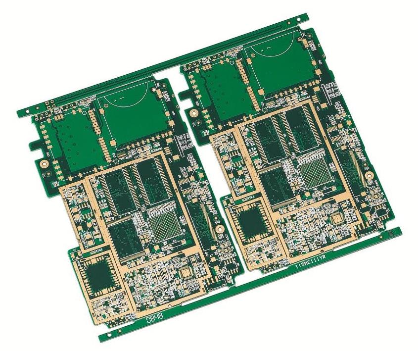
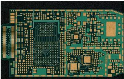
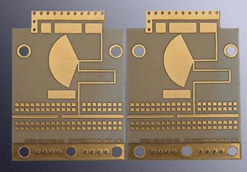
The company has a professional PCB board production team and domestic leading automated production equipment. PCB products include manufacturers, high TG boards, thick copper boards, rigid-flex boards, high-frequency boards, mixed dielectric laminates, and blinds. Buried hole boards, metal substrates and halogen-free boards.
Fast samples of high-precision circuit boards, 6-7 days for bulk orders for single and double panels, 9-12 days for 4-8 layers, 15-20 days for 10-16 layers, and 20 days for HDI boards. Double-sided proofing can be delivered in as fast as 8 hours.
Provide quick quotation of information
1. PCB Gerber file or PCB file
2. Production quantity
3. Thickness of PCB board
4. Sheet
5. Surface treatment
6. Solder mask color
7. If you need PCBA patch and foundry materials, please provide a BOM list
8. PCB copy board (please give us a sample)
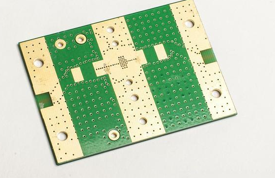
Blind vias are vias that connect the surface and inner layers without penetrating the entire board. Buried vias are vias that connect the inner layers and are not visible on the surface of the finished board. For the size settings of these two types of vias, please refer to vias. . Wire hole
The definition of the minimum hole diameter of the finished plate depends on the thickness of the plate, and the plate thickness to hole ratio should be less than 5--8.
The preferred series of apertures are as follows:
Aperture: 24mil 20mil 16mil 12mil 8mil
Pad diameter: 40mil 35mil 28mil 25mil 20mil
Inner thermal pad size: 50mil 45mil 40mil 35mil 30mil
The relationship between plate thickness and minimum aperture:
Board thickness: 3.0mm 2.5mm 2.0mm 1.6mm 1.0mm
Minimum aperture: 24mil 20mil 16mil 12mil 8mil

Test hole
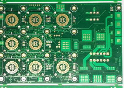
Test holes refer to vias used for ICT testing purposes, which can also be used as via holes. In principle, the aperture is not limited, the diameter of the pad should be no less than 25mil, and the center distance between the test holes should not be less than 50mil. Multilayer circuit board
Factors to be considered in the setting of the line width and line spacing of the blind hole board
A. The density of the veneer. The higher the density of the board, the tendency to use finer line widths and narrower gaps.
B. The current strength of the signal. When the average current of the signal is large, the current that the wiring width can carry should be considered
The width of the wire should be able to meet the electrical performance requirements and be easy to produce. Its minimum value is determined by the current size, but the minimum should not be less than 0.2mm. In the high-density, high-precision printed circuit, the wire width and The spacing is generally 0.3mm
PCB manufacturer-description of the structure of blind and buried vias
In terms of process, these vias are generally divided into three categories, namely blind vias, buried vias and through vias. Printed circuit boards with buried and blind hole structures are generally completed by "sub-board" production methods, which means that they must be completed through multiple pressing, drilling, and hole plating, so precise positioning is very important .
However, vias are one of the important components of multilayer PCB, and the cost of drilling usually accounts for 30% to 40% of the PCB manufacturing cost. Simply put, every hole on the PCB can be called a via.
There are three different methods for the production process of multi-layer blind vias, as described below
A, mechanical fixed depth drilling
In the traditional multilayer board manufacturing process, after pressing, the drilling machine is used to set the depth of the Z axis, but this method has several problems.
a. Only one drill at a time can produce very low output
b. The level of the drilling machine table is strictly required, and the drilling depth of each spindle must be set to be consistent, otherwise it is difficult to control the depth of each hole
c. Electroplating in the hole is difficult, especially if the depth is greater than the hole diameter, it is almost impossible to do the electroplating in the hole.