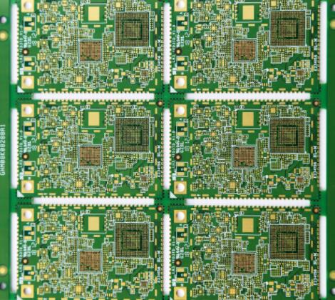
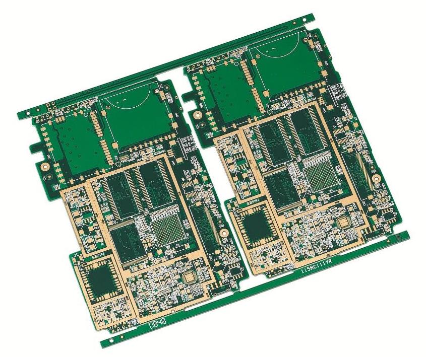
1. RF circuit board layout principle
In the design of RF PCB layout, the following general principles must be given priority to:
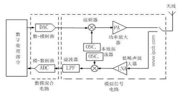
(1) The high-power RF amplifier (HPA) and low-noise amplifier (LNA) should be isolated as far as possible. In short, the high-power RF transmitting circuit should be far away from the low-power RF receiving circuit;
(2) Make sure that there is at least one whole area in the high power area of PCB board, and it is better to have no vias on it. Of course, the larger the copper foil area, the better;
(3) Decoupling of circuit and power supply is also very important;
(4) RF output usually needs to be away from RF input;
(5) Sensitive analog signals should be kept away from high-speed digital signals and RF signals as far as possible;

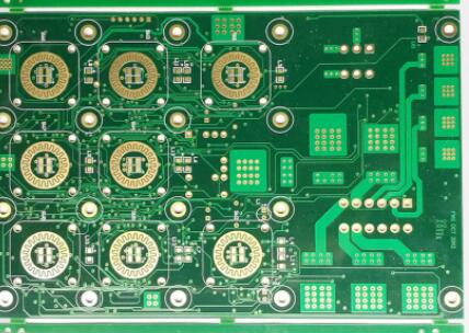
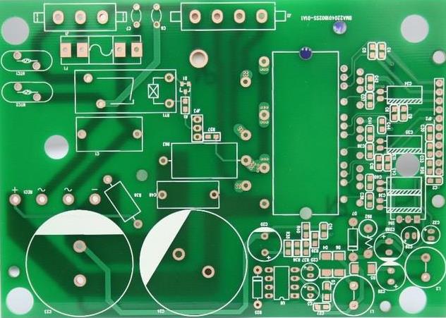
2. Physical zoning, electrical zoning, design zoning
It can be decomposed into physical partition and electrical partition. Physical zoning mainly involves the layout, orientation and shielding of components; electrical zoning can be further divided into power distribution, RF wiring, sensitive circuit and signal and grounding.
3. In the design of mobile phone PCB board, we should pay attention to several aspects
1) Treatment of power supply and ground wire:
Even if the wiring in the whole PCB board is well completed, the interference caused by the thoughtless consideration of power supply and ground wire will degrade the performance of the product, and sometimes even affect the success rate of the product.
Therefore, the wiring of electricity and ground wire should be taken seriously to minimize the noise interference generated by electricity and ground wire, so as to ensure the quality of products.
For every engineer engaged in electronic product design, they understand the causes of the noise between the ground wire and the power line
4. High frequency PCB design skills and methods
(1) 45 ° angle should be adopted at the corner of transmission line to reduce back loss.
(2) High performance insulation circuit board with insulation constant value strictly controlled by levels should be adopted. This method is conducive to the effective management of the electromagnetic field between the insulation material and the adjacent wiring.
(3) It is necessary to improve the PCB design specifications for high-precision etching. Consider specifying a total line width error of + / - 0.0007 inches, managing undercut and cross sections of wiring shapes, and specifying plating conditions for wiring sidewalls. The overall management of wiring (conductor) geometry and coating surface is important to solve the skin effect problem related to microwave frequency and realize these specifications.
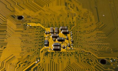
(4) Protruding leads have tapped inductors, avoid using components with leads. In high frequency environments, surface mount components are preferred.
(5) For signal vias, it is necessary to avoid the use of via processing (PTH) on the sensitive board, because this process will lead to lead inductance at the via.
(6) We should provide abundant grounding strata. These ground planes should be connected by moulded holes to prevent the influence of 3D electromagnetic field on the circuit board.
(7) To choose non electrolytic nickel plating or immersion gold plating process, do not use HASL method for electroplating.
(8) The solder mask prevents solder paste from flowing. However, due to the uncertainty of the thickness and the unknown insulation properties, the whole board surface is covered with solder mask, which will lead to a great change of electromagnetic energy in microstrip design. In general, the welding dam is used as the electromagnetic field of the solder mask.
In this case, we manage the transition from microstrip to coaxial cable. In a coaxial cable, the ground wire layers are circular and evenly spaced. In microstrip, the ground plane is below the active line.
This introduces some edge effects, which need to be understood, predicted and considered in the design. Of course, this mismatch will also lead to back loss, which must be minimized to avoid noise and signal interference.
5. EMC design
Electromagnetic compatibility refers to the ability of electronic equipment to work coordinately and effectively in various electromagnetic environments.
The purpose of electromagnetic equipment PCB design is to reduce the electromagnetic interference to other electronic equipment.