(1) Power line is an important way for EMI in and out of the circuit. Through the power line, the external interference can be transmitted into the internal circuit and affect the RF circuit index. In order to reduce electromagnetic radiation and coupling, the primary side, secondary side and load side loop area of DC-DC module are required to be minimum. No matter how complex the form of power supply circuit is, its large current loop should be as small as possible. The power cord and ground wire should always be placed close together.
(2) If the switching power supply is used in the circuit, the peripheral device layout of the switching power supply should conform to the principle of the shortest power return path. The filter capacitor should be close to the relevant pins of switching power supply. Use common mode inductor, close to switching power supply module.
(3) The long distance power line on the single board can not approach or pass through the output and input terminals of the cascade amplifier (gain greater than 45dB) at the same time. Avoid power line as RF signal transmission path, which may cause self excitation or reduce sector isolation. High frequency filter capacitor should be added at both ends of long distance power line, even in the middle.
(4) Three filter capacitors are connected in parallel at the power inlet of RF PCB. The advantages of these three capacitors are used to filter the low, medium and high frequency of power line respectively. For example: 10uF, 0.1uF, 100pF. It is close to the input pin of the power supply in order from large to small.

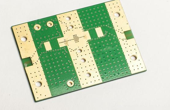
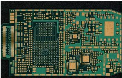
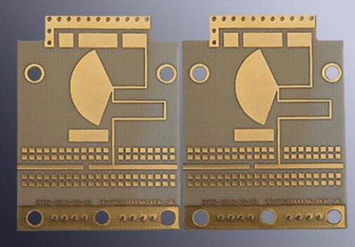
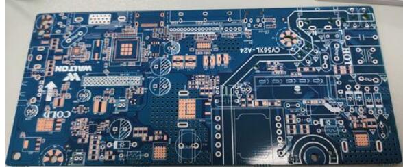
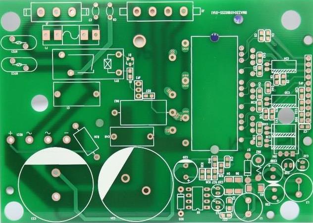
RF PCB design
(5) When using the same group of power supply to feed small signal cascade amplifier, we should start from the last stage and supply power to the front stage in turn, so that the EMI produced by the last stage circuit has little influence on the front stage. Each stage of power filter has at least two capacitors: 0.1uF, 100pF. When the signal frequency is higher than 1GHz, 10PF filter capacitor should be added.
(6) The filter capacitor should be close to the transistor pin, and the high frequency filter capacitor should be closer to the pin. The transistor with lower cut-off frequency is selected. If the triode in the electronic filter is a high-frequency transistor, which works in the amplification area, and the layout of peripheral devices is unreasonable, it is easy to produce high-frequency oscillation at the power output. The same problem may exist in the linear regulator module, because there is feedback loop in the chip, and the internal triode works in the amplification area. The high frequency filter capacitor should be close to the pin to reduce the distributed inductance and destroy the oscillation condition.
(7) The copper foil size of the power part of PCB board conforms to the maximum current flowing through it, and the allowance is considered (the general reference is 1A / mm line width).
(8) The input and output of the power line should not be crossed.
(9) Pay attention to decoupling and filtering of power supply to prevent interference of different units through power line. Power lines shall be isolated from each other during power wiring. The power line is isolated from other strong interference lines (such as CLK) by ground wire.
(10) The power wiring of small signal amplifier needs to be isolated from ground copper and grounding via to avoid other EMI interference, which will deteriorate the signal quality.
(11) Different power layers should avoid overlapping in space. In order to reduce the interference between different power sources, especially between some power sources with large voltage difference, the overlapping problem of power supply plane must be avoided. If it is difficult to avoid, the interlayer can be considered.
(12) PCB layer allocation is easy to simplify the subsequent wiring processing. For a four layer PCB (commonly used in WLAN), components and RF leads are placed on the top of the circuit board in most applications. The second layer is used as a systematic ground, the power part is placed in the third layer, and any signal line can be distributed in the fourth layer.
Continuous ground plane layout in the second layer is very necessary for the establishment of impedance controlled RF signal path. It is also convenient to obtain the shortest ground loop as possible, providing high electrical isolation for the first and third layers, so as to minimize the coupling between the two layers. Of course, other layer definitions can also be used (especially when the circuit board has different layers), but the above structure is a successful example after verification.
(13) Large area of power layer can make VCC wiring easy, but this structure is often the fuse of system performance deterioration. If all power leads are connected together on a large plane, the noise transmission between pins cannot be avoided. On the contrary, if the star topology is used, the coupling between different power supply pins will be reduced.