1, Definition of high frequency PCB
High frequency PCB refers to the special PCB with high electromagnetic frequency, which is used in the fields of high frequency (frequency greater than 300MHz or wavelength less than 1m) and microwave (frequency greater than 3GHz or wavelength less than 0.1M). It is a PCB produced by using common rigid PCB manufacturing method or using special processing methods on Microwave PCB substrate copper clad laminate. Generally speaking, high frequency PCB board can be defined as PCB board with frequency above 1GHz.
With the rapid development of science and technology, more and more equipment design is in the microwave frequency band (> 1GHz) and even in the millimeter wave field (30ghz). This also means that the frequency is higher and higher, and the requirements of PCB substrate are also higher and higher. For example, PCB substrate materials need to have excellent electrical properties and good chemical stability. With the increase of power signal frequency, the loss requirement on the substrate is very small, so the importance of high-frequency PCB board is highlighted.

2, Application fields of high frequency PCB
2.1 mobile communication products, intelligent lighting system
2.2 power amplifier, low noise amplifier, etc
2.3 power divider, coupler, duplexer, filter and other passive components
2.4 in the fields of automobile anti-collision system, satellite system and radio system, the high frequency of electronic equipment is the development trend.
3, Classification of high frequency PCB
3.1 powder ceramic filled thermosetting materials
A. Manufacturer of high frequency PCB board:
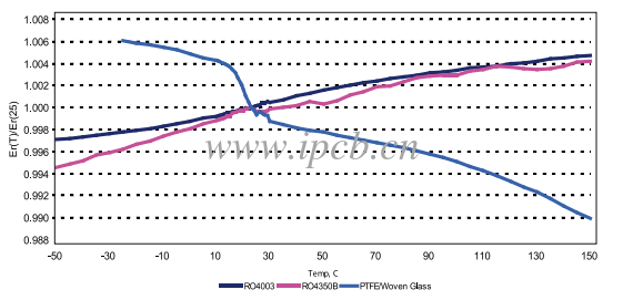
Rogers 4350b / 4003c
Arlon's 25N / 25FR
Taconic's TLG series
B. Processing method of high frequency PCB board:
The processing process is similar to that of epoxy resin / glass woven fabric (FR4), but the plate is brittle and easy to break. When drilling and punching, the service life of drill bit and Gong knife will be reduced by 20%.
3.2 PTFE material
A: Manufacturer of high frequency PCB board
1. Rogers' ro3000 series, RT series and TMM series
2. Arlon's ad / AR series, isoclad series and cuclad series
3. Taconic's RF series, TLX series and tly series
4. F4b, f4bm, f4bk, tp-2 of Taixing microwave
B: Processing method of high frequency PCB
1. Cutting of high frequency PCB board: the protective film must be reserved to prevent scratch and indentation
2. Drilling of high frequency PCB board:
2.1 a new drill bit (standard 130) is used. The best one is one piece and one stack. The pressure of presser foot is 40psi
2.2 aluminum sheet is the cover plate, and then use 1 mm melamine backing plate to tighten the PTFE plate
2.3 blow out the dust in the hole with air gun after drilling
2.4 with the most stable drilling rig, the drilling parameters (basically, the smaller the hole, the faster the drilling speed; the smaller the chip load, the smaller the return speed)
3. Hole treatment of high frequency PCB board
Plasma treatment or sodium naphthalene activation treatment is conducive to pore metallization
4. PTH copper deposition of high frequency PCB board
4.1 after micro etching (the micro erosion rate has been controlled by 20 microinch), the plate is fed from the oil cylinder after PTH pulling
4.2 if necessary, the second PTH should be passed and the plate should be fed from the expected cylinder
5. Solder mask of high frequency PCB
5.1 pretreatment: acid washing is used instead of mechanical grinding
5.2 baking plate after pretreatment (90 degree Celsius, 30min), brush green oil for curing
5.3 baking plate in three stages: 80 degree Celsius, 100 degree Celsius and 150 degree Celsius for 30min respectively (if oil is found on the surface of the substrate, rework can be carried out: wash off the green oil and reactivate it)
6. Gong board of high frequency PCB board
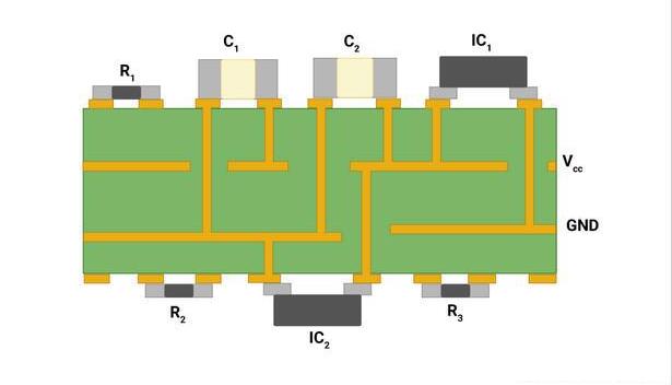
Lay the white paper on the surface of PTFE board line, and clamp it with FR-4 base plate or phenolic base plate with thickness of 1.0 mm to remove copper: as shown in the figure:
The rough edge of the back board of the Gong board needs to be carefully scraped by hand to prevent damage to the base material and copper surface, and then separated with sulfur-free paper of a certain size, and visual inspection should be carried out to reduce the burr. The key point is that the removal effect of the Gong plate process should be good.
4, Process flow of high frequency PCB
1. Npth PTFE plate processing process
Cutting - Drilling - dry film - Inspection - etching - etching - solder - character - tin spraying - forming - testing - final inspection - Packaging - Shipping
2. PTFE plate processing flow of PTH
Blanking drilling hole treatment (plasma treatment or sodium naphthalene activation treatment) - copper deposition - plate electricity dry film - Inspection - Graphic electricity - etching - Corrosion Inspection - solder mask - character - tin spraying - forming - testing - final inspection - Packaging - Shipping
5, Summary of high frequency PCB
Processing difficulties of high frequency PCB
1. Copper deposition: the hole wall is not easy to copper
2. The control of line gap and sand hole of graph rotation, etching and line width
3. Green oil process: control of green oil adhesion and green oil foaming
4. Strictly control the scratch on the board surface in each process