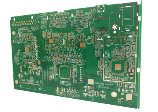
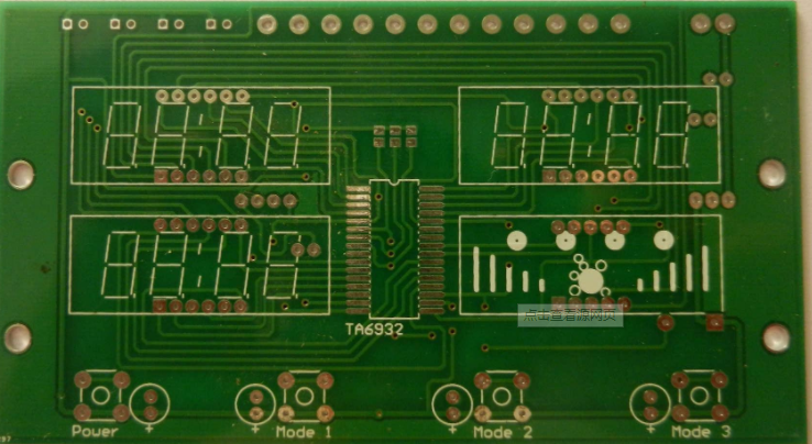
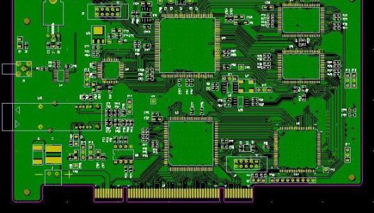
If you have the opportunity to pick up a piece of circuit board, a little look will find it has many large and small holes on printed circuit boards, bring it up to the ceiling lamp, also find many of holes, these holes where is not good-looking, each hole has its purpose and was designed.
The holes are basically PTH (Plating Through Hole) and NPTH (Non-plating Through Hole) because the holes are literally running from one side of the board to the other. In fact, in addition to the circuit board through the hole, there are other not through the hole circuit board.
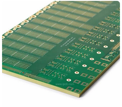
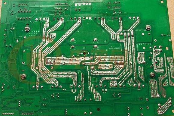
The surface of the circuit board is very porous, as shown below. It is usually divided into the following types:
1. Represents the mounting hole for separating the original
It is the installation of directly inserted (separated) components on the circuit board through certain process requirements.
2. Indicates the heat dissipation hole
This is a kind of cooling hole, and on the other side is a CPU chip.
3. Represents through hole
This hole is for connecting the front and back wires of the circuit board.
4. Indicates mounting holes
Mounting holes, as the name suggests, are used to install fixed circuit boards.
5. Holes required by other technical specifications
For example, power supply circuit boards, such as transformers, have some holes or slots to ensure technical performance requirements.

How to distinguish between PTH and NPTH through holes?
In fact, it is very simple, refer to the picture at the front of the article, just look at the hole wall has bright electroplating traces can be judged, there is electroplating traces of the hole is PTH, no electroplating traces of the hole is NPTH.
What is the use of NPTH (non-plated through hole)?
If you are careful, you will find that the aperture of NPTH is usually larger than that of PTH, because NPTH is mostly used as a lock screw, and some are used to install some external connectors.
In addition, some NPTH designs are used to test the positioning of the fixture on the break-away side, and in the early days were used to fix the circuit board for SMT.Most SMT machines now use clamps instead of thimbles to fix the circuit board.
What is the use of PTH (electroplated through hole)? What's the Via?
The PTH hole in the circuit board is used for two purposes. One is used to weld traditional dip parts. The hole diameter of these holes must be larger than the welding foot diameter of the part, so that the part can be inserted into the hole. Another smaller PTH, usually referred to as via (guide hole), is used to connect and conduction circuit board (PCB) of the copper foil line between the two layer or multilayer, because the PCB is composed of many layers of copper foil stacked accumulation, copper foil (copper) between each layer will then spread a layer of insulating layer, that is to say, the copper foil layer can't exchange between each other, Its signal is connected by via, hence the Chinese term "through-hole".
Pictured above is the profile of the side of the circuit board, think of it as a must in the ant nest, this is a six layer of copper foil in PCB, we can imagine this PCB as having like a six-storey building, each layer of copper foil represents a layer of floor, and via (guide hole) is equivalent to connecting floor stairs, and the building stairs can have several, However, not every staircase is necessarily connected to all floors. It may only connect the third and fourth floors, but nothing else. Such a stairway is called a (Buried via) Hole because you can't see any holes on the outside. Because the purpose of VIA is to conduct different layers of copper foil, it needs electroplating to conduct, so via is also a kind of PTH.
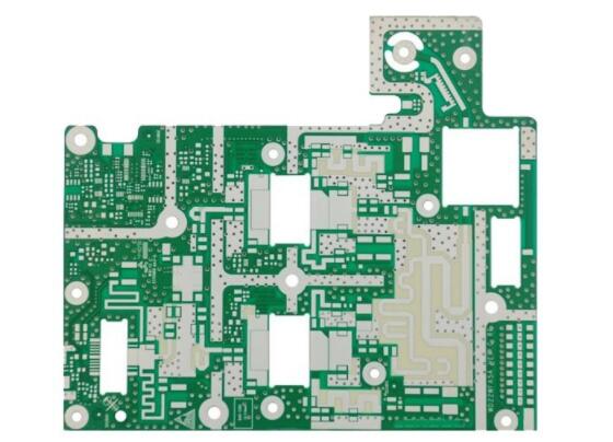
However, most via will be covered with green paint, as shown in the picture above, especially the mobile phone board. As the parts on the board become more and more dense, some via will even be placed under the parts. In order to prevent quality problems caused by accidental short circuit between the parts and via, most via will be covered with green paint. Because there will be printing solder paste on some via, when the board passes through reflow, the solder paste is likely to flow from via to the other side of the board and cause short circuit problems. Therefore, most current printed circuit board processes make the via aperture small and cover it with green paint to avoid possible quality problems in the future