Nowadays,Ku band radio frequency communication, more and more information is carried by media, especially high-definition multimedia video streams, which require more and more real-time information transmission. These demands promote the gradual increase of the information transmission rate. At present, wireless communication technology is booming, and LTE and 5G technology come one after another. According to Shannon's theorem, the rate of wireless communication is correlated with the channel bandwidth. The wider the bandwidth, the higher the rate and the larger the capacity. In the lower frequency bands such as VHF, UHF, L, and S, the spectrum resources are crowded and the available bandwidth is limited. Therefore, the development of higher frequency bands to obtain wider channel bandwidth is an inevitable trend of future communication system development.
1. System scheme design
The Ku band radio frequency communication system proposed in this paper uses beamforming technology to cover the full 360° range with a 4-plane array antenna distributed at 90°. Each antenna array is composed of 4 array elements, which are connected with 4 TR components respectively. After amplitude and phase weighting, they are collected into the same frequency conversion channel to form a 4*4 RF MIMO system. Public resources and upper management are all centralized in a central unit to facilitate interconnection. In the vehicle type structure, the central unit is connected to the TR components through connectors for signaling interaction control, and each TR component has an independent baseband processing unit, which can also send the digital if to the CENTRAL processor for centralized processing (to achieve spatial diversity).
Compared with the traditional single receiving single system, this system scheme is based on military tactics application of anti-interference and secrecy, high speed, large capacity, adaptive overall demand, the comprehensive considerations Ku band signal wavelength itself, directional strong, large transmission loss adverse factors, such as the mainstream of OFDM modulation technology, and makes the system stronger anti-jamming ability, At the same time, high-frequency spectrum utilization can be obtained. MIMO and smart antenna technology are adopted to make reasonable use of the performance of beam diversity and antenna spatial multiplexing so that the system can support multi-user, multi-direction, adaptive large-capacity data transmission as far as possible, and can be effective. Resist the influence of multipath fading on system performance during signal transmission.

Overall system block diagram
2. Subsystem scheme design
2.1 Antenna Design
To reduce the overall profile of the system, a uniform linear array microstrip antenna is used in the antenna part. The array beamforming technology can be used to achieve high directivity, wide-coverage, and anti-fading. This type of antenna design can realize multi-sector scanning by amplitude/phase weighting of the excitation source of the antenna array element. In addition, direction-finding of interference sources can be realized. If interference is detected, the antenna pattern can form a zero trap in the interference direction through beam shaping to suppress interference.
2.2 Transceiver Link Design
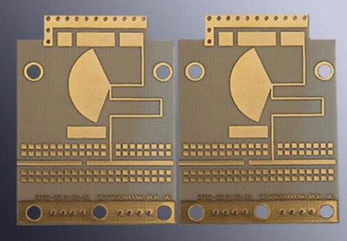
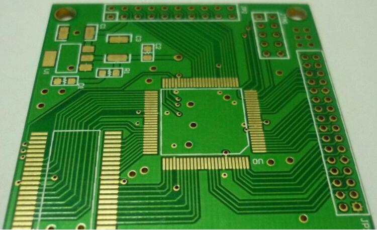
Transceiver link including TR component and variable frequency channel can be tailored according to requirements, in the microwave RF front-end adopted digital phase-shifting attenuator, in frequency conversion circuit, the superheterodyne second inverter circuit, mixing way as the high low-frequency vibration, decrease the difficulty of the realization of the frequency synthesizer and circuit design of the AGC control circuits and protective isolation circuit, The frequency selection circuit performs frequency selection, frequency conversion, linearization and amplification of the received signal, and finally provides it to the baseband processor for signal demodulation.

Preliminary layout of the system
2.3 Frequency synthesizer design
In general, there are three types of frequency synthesis available: direct frequency synthesis (DS), indirect frequency synthesis (PLL), and direct digital frequency synthesis (DDS).
This through the scheme design of frequency synthesizer using DDS with PLL frequency doubling frequency point source mixing achieve the ultimate source of frequency hopping a boost output, and receiving and launch phase calibration reference source is directly used the PLL frequency hopping and way of realization, the total frequency source synthesis scheme, the scheme of the whole idea is to crystal vibration signal of four-power splitters divided into four roads, One signal was used as the clock of transmitting and receiving phase calibration reference frequency source, and the C-band signal was generated by PLL frequency hopping locking, and then the Ku-band reference frequency source was output by filtering and double frequency doubling. The other signal serves as the reference clock of the baseband processor; The third signal, as the reference clock of the C-band point frequency source, is locked by PLL to generate the C-band point frequency signal, and then mixed with the FH signal output by DDS to generate the up-conversion C-band radio frequency signal, and then the second frequency doubling to generate the x-band first vibration signal. Finally, one signal is used as the reference clock of the l-band point frequency source, which is locked by PLL to generate an l-band point frequency signal. Then, the power is divided into two ways. One way is used as the two local oscillators of the system through filtering and amplification, and the other way is used as the reference clock of fH DDS to generate fH signal in the VHF band. After filtering, amplification, and double frequency, the l-band fH signal is generated and the c-band point frequency source is mixed, filtered, amplified, and doubled to produce X-band first vibration signal. In the process of frequency source realization, because it involves many PLL frequency synthesis, frequency multiplication, mixing, amplification, and other circuits, so the stray suppression or avoidance in the process of radio frequency communication conversion is particularly important, otherwise, the interference of stray signals will affect the communication quality of the system.

Schematic diagram of antenna array and main and sub-office scanning
At present, the commonly used heat dissipation methods in engineering include fin heat dissipation, phase change cooling, heat pipe heat transfer, thermoelectric refrigeration, and so on. The most used heat dissipation method is fin heat dissipation teeth, according to the different structures of heat dissipation teeth can be divided into plate type heat dissipation teeth and column type heat dissipation teeth. Pillar radiator tooth duct is not closed, the cooling effect is better than chip cooling tooth is obvious, therefore, in this system used the chip cooling of cooling methods, theoretical cooling tooth, the higher the cooling effect is better, but the width of the tooth itself and tooth spacing will also have an impact on heat dissipation effect, its cooling effect can be through thermal design software to simulation optimization (Flotherm). The heat dissipation teeth are made of aluminum to meet the requirement of weight reduction.
In addition to the above auxiliary heat dissipation design strategy, thermal grease and thermal glue are also added to the bottom of the power amplifier in the project. Meanwhile, each T/R component is distributed to reduce the concentration of heat sources and enhance the reliability of the system.

Principle block diagram of frequency synthesizer
3. Engineering design verification
According to the system design scheme, we test the antenna, the frequency synthesizer engineering test results are similar to the design, the typical frequency synthesizer DDS+PLL phase noise and radio frequency communication hopping time test curve
When the intermediate frequency input is 140MHz modulation signal, the modulation mode is 64QAM, the roll drop factor is set to 0.3, and the symbol rate is 30Mbps, the typical transmitting EVM is 6.09%.
4. Application scenario
At present, a high-speed broadband radio frequency communication system based on Ku band is mainly applied in the fields of point-to-point, point-to-multipoint, relay, and multistage AD network, which can greatly expand the performance and system capacity of node communication.