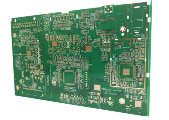
Although there are still many theoretical uncertainties in RF circuit board design, there are still many rules that can be followed in RF board design. However, in practical design, the really useful technique is how to compromise these rules when they are not implemented due to various limitations. This article will focus on the various issues related to the design of RF circuit board partitions.
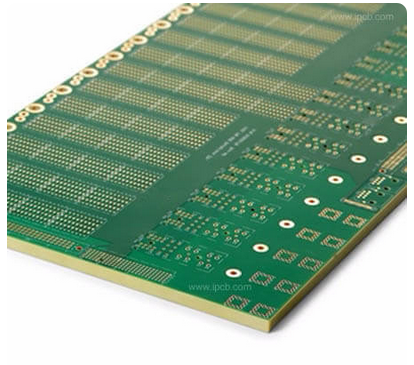
The different properties of the circuit on the board must be separated, but connected in optimal conditions without electromagnetic interference, which requires microvia. Generally, the diameter of micro holes is 0.05mm~0.20mm, and these holes are generally divided into three categories, namely blind via, bury via and through VIA. Blind holes are located on the top and bottom surfaces of the printed circuit board and have a certain depth for connecting the surface circuit to the inner circuit below. The depth of the holes usually does not exceed a certain ratio (aperture). Buried holes are connection holes in the inner layer of the printed circuit board that do not extend to the surface of the printed circuit board. Both types of holes are located in the inner layer of the circuit board, which is completed by the through-hole molding process before lamination, and several inner layers may be overlapped during the formation of the through-hole. The third type, called through-holes, runs through the entire circuit board and can be used for internal interconnections or as adhesive positioning holes for components.

1. Use partitioning techniques
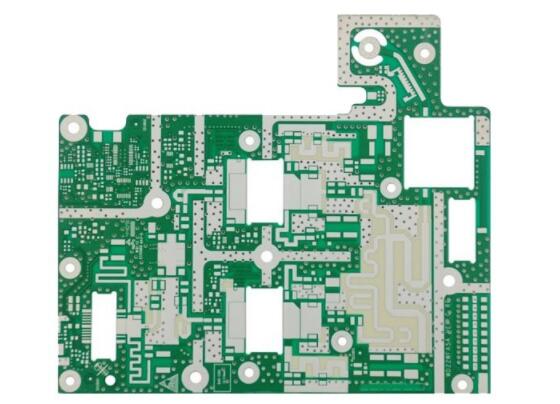
In the design of RF circuit board, should be as far as possible to the high power RF amplifier (HPA) and low noise amplifier (LNA) isolated, simple to say, is to let the high power RF transmitting circuit away from the low noise receiving circuit. This can be done easily if there is a lot of space on the PCB. But usually with a lot of components, the PCB manufacturing space becomes very small, so this is difficult to achieve. You can place them on both sides of the PCB, or have them work alternately rather than simultaneously. High power circuits may also sometimes include RF buffers (buffers) and voltage controlled oscillators (VCO).
2. Entity partitioning
Component layout is the key to achieving an excellent RF design. The most effective technique is to first fix the component on the RF path and Orient it to minimize the length of the RF path. And keep RF input away from RF output, and as far as possible away from high power circuits and low noise circuits.
In physical space, linear circuits such as multistage amplifiers are usually sufficient to isolate multiple RF regions from each other, but diplexers, mixers, and IF amplifiers always have multiple RF/IF signals interfering with each other, so care must be taken to minimize this effect. RF and IF cables should be crossed as far as possible, and a ground area should be separated between them as far as possible. The correct RF path is very important to the performance of the entire PCB, which is why component layout usually takes up most of the time in mobile phone PCB design.
On a mobile phone PCB, it is usually possible to place a low noise amplifier circuit on one side of the PCB pattern and a high power amplifier on the other, and eventually connect them to one end of the RF antenna and the other end of the base frequency processor on the same side by means of a dipper. This requires some skill to ensure that RF energy is not transferred from one side of the board to the other through holes, a common technique is to use blind holes on both sides. The adverse effects of passing holes can be minimized by arranging blind holes in areas on both sides of the PCB that are free from RF interference.
3. Metal shield
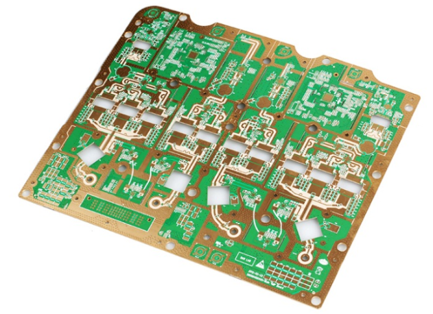
In some cases, it is not possible to retain sufficient separation between multiple circuit blocks, in which case metal shields must be considered to shield RF energy within the RF region. However, metal shields also have side effects, such as high manufacturing and assembly costs.
It is difficult to ensure high precision of metal shield with irregular shape in manufacturing, and the layout of components is limited by rectangular or square metal shield. Metal shield is not conducive to component replacement and fault shift; Because the metal shield must be welded to the ground surface and kept at an appropriate distance from the components, it takes up valuable PCB space.
It is important to ensure the integrity of the metal shield as much as possible, so the digital signal lines entering the metal shield should go through the inner layer as much as possible, and it is best to set the next layer of the signal line layer as the ground layer. RF signal line can go out from the small gap at the bottom of the metal shield cover and the wiring layer of the grounding gap, but the gap should be surrounded by a large grounding area as far as possible, the grounding of different signal layer can be connected by a plurality of holes. Despite these disadvantages, metal shields are still very effective and are often the only solution for isolating critical circuits.

4. Power supply decoupling circuit
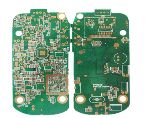
Appropriate and effective chip power decoupling (PPLE) circuits are also important. Many RF chips with integrated linear circuits are very sensitive to power source noise, and typically each chip requires up to four capacitors and an isolating inductor to filter out all power source noise.
The physical location of these decoupled components is also often critical. Several important component layout principle is: the C4 as far as possible close to the IC pins and grounding, C3 must be the most close to the C4, C2 must be the most close to C3, and the connection of the foot and C4 of IC go line should be as short as possible, that the grounding end of the several components (especially the C4) usually should borrow an board face down the ground plane and ground connected to the foot of the chip. The through-hole connecting the assembly to the ground layer should be as close as possible to the assembly pad on the PCB. It is best to use a blind hole on the pad to minimize the inductance of the connection line, L1 should be close to C1.
An integrated circuit or amplifier usually has an open collector output, so a pullup inductor is required to provide a high impedance RF circuit board load and a low impedance DC power supply. The same principle applies to decoupling the power side of this inductor. Some chips require more than one power supply to work, so it may take two or three sets of capacitors and inductors to decouple them separately, which may not work well if there is not enough space around the chip. In particular, the inductors are rarely parallel to each other, since this would form a hollow-core transformer and induce interference signals, so they must be at least as far apart as one of the heights, or arranged at right angles to minimize mutual inductance.