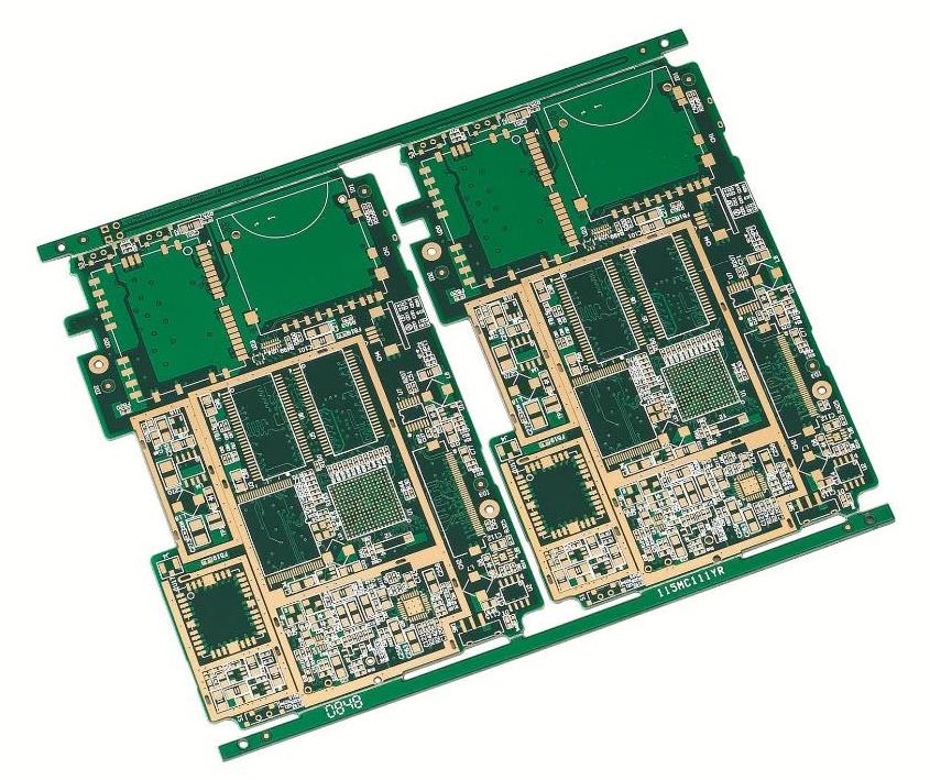
The operating frequency of 5G will be much higher than that of 4G, forcing PCB designers to reconsider their PCB board design and manufacturing methods.
With the advent of 5G, electrical engineers must reconsider (and sometimes redesign) their PCBs and other infrastructure to support the high frequencies of the new spectrum. Signal integrity will become the primary issue in the design of 5G PCB boards.
5G's position on the electromagnetic spectrum
In this article, let us look at the impact of higher frequencies on PCB signal integrity and ways to alleviate these problems.

Why is 5G frequency bad for signal integrity?
In circuit board design, an increase in frequency will have many undesirable effects on signal integrity--especially the effects of increased noise and attenuation.
Noise
Regarding noise, the first thing to consider is that as the system frequency increases, signal reflection becomes more and more important. According to transmission line theory, reflection is directly related to the ratio of transmission line length to signal wavelength.
Signal reflection
We also know that the signal wavelength decreases as the frequency increases (λ = v / f). Therefore, as 5G introduces higher frequencies, designers must also consider the effects of signal reflections, such as ringing or other distortions, which will cause more noise in the system and effectively reduce SNR.
Capacitive and inductive coupling
In addition, since capacitance and inductance are related to the rate of change of voltage and current, respectively, the effects of capacitive coupling and inductive coupling become more relevant. This also generates noise and distortion, which reduces SNR.
Attenuation and skin effect
Regarding attenuation, an important consideration is the so-called skin effect. It essentially shows that as the frequency of the signal increases, the penetration depth of the signal in the conductor decreases.
Skin effect
The important meaning of the skin effect is that as higher frequencies pass through a smaller area, they will encounter greater resistance and cause greater IR loss. This loss also reduces SNR.
Ways to improve SNR in 5G design
In high-speed design, there are many factors that affect signal integrity. So, what can designers of 5G PCB boards do?
Control circuit board impedance
An important step to reduce signal reflection and attenuation is to control the impedance of the circuit board. Having properly terminated wiring and a well-designed impedance matching network is essential to prevent signal reflections and provide maximum power to the circuit module.
Focus on impedance in manufacturing: mSAP
The impedance control problem can also be solved when manufacturing circuit boards. The traditional PCB manufacturing process has the disadvantage of creating traces with trapezoidal cross-sections. These cross sections will change the impedance of the trace itself, which severely limits 5G applications.
One solution is to use mSAP (semi-additive manufacturing process) technology, which allows manufacturers to create traces with higher accuracy. The geometry of the control circuit can also help alleviate the skin effect and the signal power loss caused by it.
Subtraction and mSAP process. Image courtesy of Proto-Electronics
Place components and traces
When mitigating effects such as coupling, the most important thing is to wisely connect components and traces to each other and to ground. For example, a multi-layer PCB with a buried ground plane and power plane may be a useful solution.
Placing sensitive lines near the ground plane forces capacitive coupling with ground (as opposed to other lines) and provides a low-inductance return path for high-speed signals.
More considerations for 5G design
Although this article does not address an exhaustive list of all issues or solutions, we reviewed some of the advanced issues of signal integrity in 5G frequencies and possible design solutions to solve these issues.
Obviously, 5G will bring signal integrity challenges to PCB engineers, because the frequency-dependent effects of noise and attenuation will reduce SNR. For a successful 5G design, some factors not considered in this article (such as the choice of dielectric and substrate materials) are equally important.