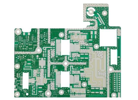
Analysis of the influence of materials and processing on PCB circuit Dk and phase consistency
As the frequency continues to increase, it becomes more and more difficult to control the phase consistency of printed circuit board(PCB) materials. Accurately predicting the phase change of circuit board materials is not a simple or routine task. The signal phase of a high-frequency and high-speed PCB depends to a large extent on the structure of the transmission line processed from it and the dielectric constant (Dk) of the circuit board material. The lower the Dk of the medium is (for example, the Dk of air is about 1.0), the faster the electromagnetic wave propagates. As Dk increases, the propagation of the wave will slow down, and this phenomenon will also have an impact on the phase response of the propagating signal. When the Dk of the propagation medium changes, the waveform phase will change, because a lower or higher Dk will make the speed of the signal in the propagation medium faster or slower.
The Dk of circuit board materials is usually anisotropic, with different Dk values in the three dimensions (3D) of length, width, and thickness (corresponding to the x, y, and z axes). For some special types of circuit design, not only the difference in Dk needs to be considered, but also the influence of circuit processing and manufacturing on the phase. With the increase of PCB operating frequency, especially at microwave and millimeter wave frequencies, such as: fifth-generation (5G) cellular wireless communication network infrastructure equipment, advanced driver assistance systems (ADAS) in electronic assisted vehicles, phase The stability and predictability will become more and more important.

So what caused the Dk of the circuit board material to change? In some cases, the difference in Dk on the PCB is caused by the material itself (such as changes in copper surface roughness). In other cases, the PCB manufacturing process will also cause changes in Dk. In addition, the harsh working environment (such as higher working temperature) will also change the Dk of the PCB. Through understanding the characteristics of materials, manufacturing processes, working environment, and even Dk testing methods, how to study the changes in PCB Dk. This can better understand and predict the phase change of the PCB, and minimize its impact.
Anisotropy is an important characteristic of circuit board materials, and the characteristic of Dk is very similar to the "tensor" in three-dimensional mathematics. The different Dk values on the three axes result in the difference of electric flux and electric field strength in three-dimensional space. According to the type of transmission line used in the circuit, the phase of the circuit with the coupling structure can be changed by the anisotropy of the material, and the performance of the circuit depends on the direction of the phase on the circuit board material. Generally speaking, the anisotropy of the circuit board material will vary with the thickness of the board and the operating frequency, and the material with a lower Dk value is less anisotropy. Filled reinforcing materials can also cause this change: compared to circuit board materials without glass fiber reinforcement, circuit board materials with glass fiber reinforcement generally have greater anisotropy. When the phase is the key indicator and the Dk of the PCB is part of the circuit design modeling, the description and comparison of the Dk value between the two materials should be for the Dk on the same axis. For more detailed information on the various factors (including measurement methods) that change the Dk of circuit board materials, please refer to Rogers"webinar "Understand How circuit Materials and Fabrication Can Affect PCB Dk Variation and PhaseConsistency" How does the manufacturing process affect the PCB's Dk change and phase consistency)".
In-depth discussion of design Dk
The effective Dk of a circuit depends on how electromagnetic waves propagate in a specific type of transmission line. Depending on the transmission line, part of the electromagnetic wave propagates through the dielectric material of the PCB, and the other part propagates through the air around the PCB. The Dk value of air (approximately 1.00) is lower than any circuit material. Therefore, the effective Dk value is essentially a combined Dk value, which consists of electromagnetic waves propagating in the transmission line conductor, electromagnetic waves propagating in dielectric materials, and propagating in the air around the substrate Determined by the combined action of electromagnetic waves. "Design Dk" attempts to provide a more practical Dk than "effective Dk", because "Design Dk" also considers the comprehensive effects of different transmission line technologies, manufacturing methods, wires, and even test methods for measuring Dk. The design Dk is the Dk extracted when the material is tested in the circuit form, and it is also the Dk value most suitable for use in circuit design and simulation. The design Dk is not the effective Dk of the circuit, but it is the material Dk determined by measuring the effective Dk. The design Dk can reflect the true performance of the circuit.
The surface roughness of the conductor copper foil in different thicknesses of the PCB dielectric material has different effects on the design Dk and the phase response of the circuit. Materials with thicker substrates tend to be less affected by the surface roughness of copper foil conductors. Even for copper foil conductors with rougher surfaces, the design Dk value at this time is closer to the dielectric Dk of the substrate material. For example, Rogers' 6.6 mil RO4350B™ circuit board material has an average design Dk value of 3.96 from 8 to 40 GHz. For the same material with a thickness of 30 mils, the design Dk drops to 3.68 on average in the same frequency range. When the thickness of the material substrate is doubled again (60 mils), the design Dk is 3.66, which is basically the inherent Dk of the medium of this glass fiber reinforced laminate.
It can be seen from the above examples that the thicker dielectric substrate is less affected by the roughness of the copper foil, and the design Dk value is relatively lower. However, if thicker circuit boards are used to produce and process circuits, especially at millimeter wave frequencies where the signal wavelength is small, it will be more difficult to maintain the consistency of signal amplitude and phase. Circuits with higher frequencies are often more suitable for thinner circuit boards, and the dielectric part of the material has less impact on the design Dk and circuit performance at this time. Thinner PCB substrates will be more affected by conductors in terms of signal loss and phase performance. At millimeter wave frequencies, as far as the design Dk of circuit materials is concerned, they are more sensitive to conductor characteristics (such as copper foil surface roughness) than thicker substrates.
How to choose a transmission line circuit
At RF/microwave and millimeter wave frequencies, circuit design engineers mainly use the following conventional transmission line technologies, such as: microstrip line, strip line, and grounded coplanar waveguide (GCPW). Each technology has different design methods, design challenges, and related advantages. For example, the difference in GCPW circuit coupling behavior will affect the circuit design Dk. For tightly coupled GCPW circuits and closely spaced transmission lines, using the air between the coplanar coupling regions can achieve more efficient electromagnetic propagation and reduce losses. To the lowest. By using thicker copper conductors, the sidewalls of the coupling conductors are higher, and the use of more air paths in the coupling area can minimize circuit losses, but it is more important to understand the corresponding changes brought about by reducing the thickness of the copper conductor Impact.
Many factors can affect the design Dk of a given circuit and board material. For example, the temperature coefficient Dk (TCDk) of the circuit board material is used to measure the influence of the operating temperature on the design Dk and performance. A lower TCDk value indicates that the circuit board material has less temperature dependence. Similarly, high relative humidity (RH) will also increase the design Dk of circuit board materials, especially for materials with high moisture absorption. The characteristics of the circuit board material, the circuit manufacturing process, and the uncertain factors in the working environment will all affect the design Dk of the circuit board material. Only by understanding these characteristics and fully considering these factors in the design process can their impact be minimized.