BGA pad design standard and basic rules
The packaging structure of BGA devices can be divided into two types according to the shape of solder joints: spherical solder joints and cylindrical solder joints. BGA packaging technology uses round or cylindrical solder joints hidden under the package, which is characterized by large lead spacing and short lead length.

BGA Points
BGA pad design
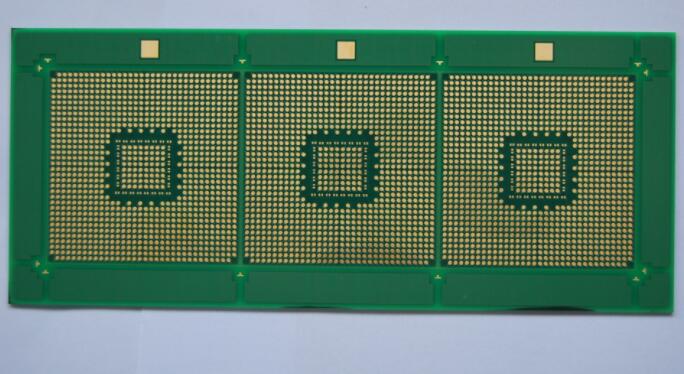
According to statistics, in surface mount technology, 70% of welding defects are caused by design reasons. BGA: roll assembly technology is no exception. With the miniaturization of the solder ball diameter of BGA chip to 0.5mm, 0.45mm and 0.30mm, the size and shape of the pad on the printed board are directly related to the reliable connection between BGA chip and the printed board, and the impact of pad design on the solder ball welding quality is also gradually increasing. The same BGA chips (ball diameter 0.5 mm, spacing 0.8 mm) are welded on printed board pads with diameters of 0.4 mm and 0.3 mm respectively by the same welding process. The verification results show that the proportion of BGA false soldering in the latter is as high as 8%. Therefore, BGA pad design is directly related to the welding quality of BGA. The standard BGA pad design is as follows:
A. Solder resist design
Design form 1: the solder resist layer surrounds the copper foil pad and leaves a gap; All leads and vias between pads shall be soldered.
Design form 2: the solder resist layer is on the pad, and the diameter of the pad copper foil is larger than the size of the solder resist opening.
In the design of these two solder resist layers, the first design form is generally preferred. Its advantages are that the diameter of copper foil is easier to control than the size of solder resist, the stress concentration of BGA Solder joint is small, and the solder joint has sufficient space settlement, which increases the reliability of solder joint.
B. Pad design graphics and dimensions
The BGA pad and via are connected by printed wire, and the via is not directly connected with the pad or directly opened on the pad.

BGA Design
General rules for BGA pad design:
(1) Pad diameter can not only affect the reliability of solder joints, but also affect the wiring of components. The pad diameter is usually smaller than the ball diameter. In order to obtain reliable adhesion,
Generally reduced by 20% - 25%. The larger the pad, the smaller the wiring space between the two pads. For example, the BGA package with a spacing of 1.27mm adopts a pad with a diameter of 0.63mm. Two wires can be arranged between the pads, with a line width of 125 microns. If a pad diameter of 0.8 mm is used, only one wire with a line width of 125 microns can be passed.
(2) The following formula gives the calculation of the number of wiring between two pads, where p is the package spacing, D is the pad diameter, n is the number of wiring and X is the linewidth. P-D≥(2n+1)x
(3) The general rule is that the pad diameter on PBGA substrate is the same as that on PCB.
(4) The pad design of CBGA shall ensure that the template opening makes the solder paste leakage ≥ 0.08mm3. This is the minimum requirement to ensure the reliability of the solder joint. Therefore, the pad of CBGA is larger than that of PBGA