In the field of wireless communication, many different package integration solutions have been developed, including chip stacking technology, package on package, package in package and other forms of application system integrated packaging (SiP) . These technologies have been successfully applied in flash memory products, graphics processors, and digital signal processors, and their applications in the field of radio frequency are also getting more and more research.
RF modules are products with transmitting and/or receiving functions, which include but are not limited to passive devices, RFICs, power amplifiers (PA), switching devices, voltage regulators, crystals, etc. Compared with passive devices, active devices such as RFIC/ASIC/BB/MAC are relatively small in size. Therefore, the integration of passive components (RCL, filter, balun, matcher, etc.) has an important impact on the size of the entire module or package.
Currently, there are mainly three types of packaging carriers used in RF modules. The first type is laminated substrates, which are used in basic power amplifier devices due to their low price, mature manufacturing process, and good thermal and electrical properties. Laminated substrates have been most widely used in various modules and packages.
The second is the low-temperature co-fired ceramic (LTCC) technology, which uses ceramic as a substrate/carrier. Because of its multi-layer structure, thick metal and high dielectric constant, high quality factor (Q) inductance and large enough capacitance can be embedded in LTCC.
The third type is a thin film (TF) passive device formed on silicon or gallium arsenide, which is made using a well-known semiconductor process. These devices are sometimes referred to as integrated passive devices (IPD). They not only have small parasitic effects and electrical performance fluctuations, but also have higher capacitance. This characteristic paved the way for its application in smaller module packages.
The original RF module used the wire bonding of a single chip as the main interconnection method. Today, wire bonding, reverse soldering, and multi-chip stacking are used in RF modules at the same time. Each of the above modules uses a variety of interconnection methods, and each solution has its advantages and disadvantages. This article will introduce these different packaging solutions separately.
Laminated substrate package
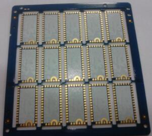
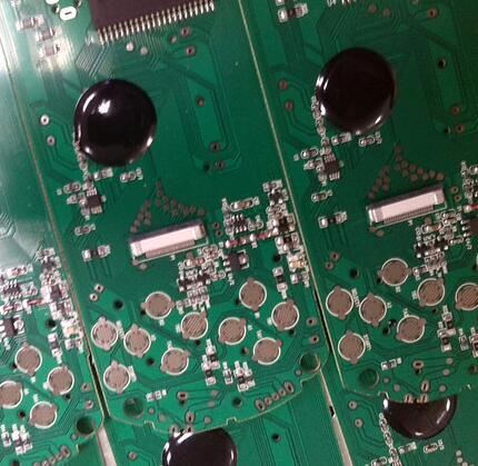
Laminates are commonly referred to as printed circuit boards(PCBs), which have been widely used in package carriers, and they still firmly occupy a large share of packaged products. Generally speaking, only two to four layers are sufficient for RF module packaging. As shown in Figure 1, the stacked module product, two chips are reverse-soldered on a four-layer laminate substrate. At the same time, 0201 surface mount (SMT) devices are also mounted in SiP applications, and the second-level circuit board connection uses BGA set up.
Chip stack packaging has been very successfully used in flash memory, photography and digital IC products. In the flash memory market, we have seen a vertical stack of multi-layer chips (7 to 8) connected by gold wire bonding. This packaging technology greatly reduces the size of the module, thereby reducing the cost of the application product.
However, in the RF packaging process, it is necessary to consider preventing the degradation of RF performance, especially the parasitic effects caused by the packaging, such as self-induction of wire bonding, and interference between the chip and the circuit board in the reverse soldering method. These packages for low-frequency and digital products may not be a problem, but it does affect the RF performance of the RFIC chip and must be considered in the package design. This effect can usually be modeled using RCL circuits and passive components. For the three-dimensional characteristics of the package, electromagnetic (EM) simulation tools can be used to derive these models.
These models can be used with chip models to test the overall electrical performance. An RF package is usually dedicated to a single application. Therefore, system-level design verification is required for a new package, including its own IC model and its parasitic package model.
Low temperature co-fired ceramic module package
LTCC technology uses a multilayer structure to implement passive components, such as RCL or corresponding functional blocks. The thickness of the dielectric layer of each layer ranges from 20um to 100um, and the total stack thickness of 10-20 layers ranges from 0.5mm to 1mm. The dielectric constant of each layer is generally 7.0 to 11.0. Inductance is usually realized through a spiral allowed by design rules. With the magnitude of the inductance, it may sometimes pass through many layers. Capacitors are also made in multiple layers and can have larger capacitance values. Thin-film barriers can also be added between ceramic layers to make resistors.
In a multilayer structure, inductors made of spiral and thick metal layers can have a higher Q value. When the operating frequency is 1.0 GHz to 6.0 GHz, the LTCC package can generally easily reach 30.0~50.0, which makes it easy to achieve low-loss RF filters on the LTCC substrate. The sandwich capacitor realized by the LTCC multilayer structure can provide sufficient capacitance for the RF system, while having a higher breakdown voltage and better ESD performance.
There are many applications that can use LTCC as a substrate package. LTCC devices can be used alone as stand-alone components, such as surface mount devices (SMT) in SiP applications. Large LTCC substrates can also be used as carrier substrates, passive devices can be embedded, and input and output connections in the form of LGA or QFN are provided. Due to its good thermal conductivity, power amplifier devices often use LTCC as a substrate.

Use integrated passive device packaging
a. Integrated passive device (IPD) as a device in SiP
In the two packaging schemes mentioned above-laminated substrate and LTCC substrate, the size of the former is relatively large because it is impossible to embed many passive components in the substrate, especially large-capacity capacitors; the latter is relatively speaking Enough inductance and capacitance with high quality factor can be made in the substrate.
The current trend is to make smaller and smaller passive devices and continue to reduce the overall size of modules or packages. So far, thin-film device technology-whether on a silicon substrate or a gallium arsenic substrate-is still the technology with the highest capacitance density. Table 1 compares the capacitance density of the three technologies.
For a 56pF capacitor, in terms of pins, size, and thickness, thin-film devices are more competitive than discrete devices. The smaller form factor makes thin-film integrated passive devices more suitable for RF modules and SiP applications. For larger-capacity capacitors (for example, greater than 100pF), discrete devices still have size advantages, and large-capacity capacitors will also be mounted on the circuit board in the form of SMT. 01005 SMT devices have appeared in the market. These shrinking devices make the package size smaller, but their prices are quite high, thereby increasing the cost of the package.
By choosing an appropriate substrate and using a thick metal layer (such as 8um), high-Q inductors can be fabricated in IPDs. Most semiconductor manufacturers understand the production process of IPD, and this process has a higher cost performance.
Radio frequency functional blocks using thin-film device technology, such as filters, diplexers, baluns, etc., take full advantage of the advantages of small form factor, so they can be widely used in manufacturing small and compact RF module or package. The capacitance density shown in Table 1 shows that whether a silicon substrate or a gallium arsenic substrate is used, integrated passive devices may be used to make the smallest package.
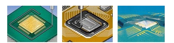
b. Chip size module package (CSMP)
The packaging technology trend is to make the module or SiP smaller and more powerful. Passive devices made by IPD technology are candidates for higher integration due to their small form factor. The wafer-level integration removes the need for traditional carrier substrates, and the integrated RCL and RF functional blocks are close to the chipset. This not only reduces the package size, but also has smaller parasitic effects and better electrical performance.
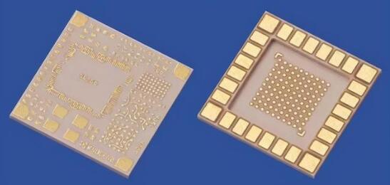
At STATS ChipPAC, we have developed a new technology that uses a large IPD/silicon carrier as the backplane structure to carry other integrated circuits (RFIC and/or BBIC) and surface mount devices. All circuit connections, filters, and baluns are made in the IPD/silicon carrier. The module consists of a large IPD chip (10mm*10mm*0.25mm) as the bottom plate, and the RFIC and BBIC are flip-chip welded on the bottom plate. The solder balls are arranged along both sides, and the height of the balls should be large enough to leave enough space for flip-chip soldered chips on the IPD.
As modules become smaller, components and circuits are compressed in a smaller area. In other words, the gap of the device circuit is smaller. In this integration mode, the integrity of the signal sometimes becomes a problem. Electromagnetic simulation tools can be used to analyze key circuit and wiring interference, so that the electrical performance of the packaged product can be guaranteed before it is finally manufactured.
For example, in a package with both RF and baseband chips (CSMP module), the mutual interference between the transmit (TX) and receive (RX) channels, and the mutual interference between the receive (RX) channel and the main baseband clock All interference must be verified by electromagnetic simulation. Minimizing the interference generated by the latter is particularly critical, because the baseband main frequency clock harmonics may fall in the radio frequency passband, thereby concealing the already weak received signal in wireless communication.
Concluding remarks
The stack package has the advantages of low cost, easy manufacturing, and good thermal and electrical performance. It is suitable for almost all radio frequency modules; the LTCC package has passive components built into the substrate, and a smaller overall size, and high Q value inductance and Large capacitors can also be built into the LTCC substrate. In addition, good thermal characteristics make LTCC widely used in power amplifier device packaging; IPD has a small form factor and is very suitable for RF module packaging. As the carrier of IPD technology, CSMP can provide the most integrated package. Both RFIC and BBIC can be integrated in a small package using CSMP.