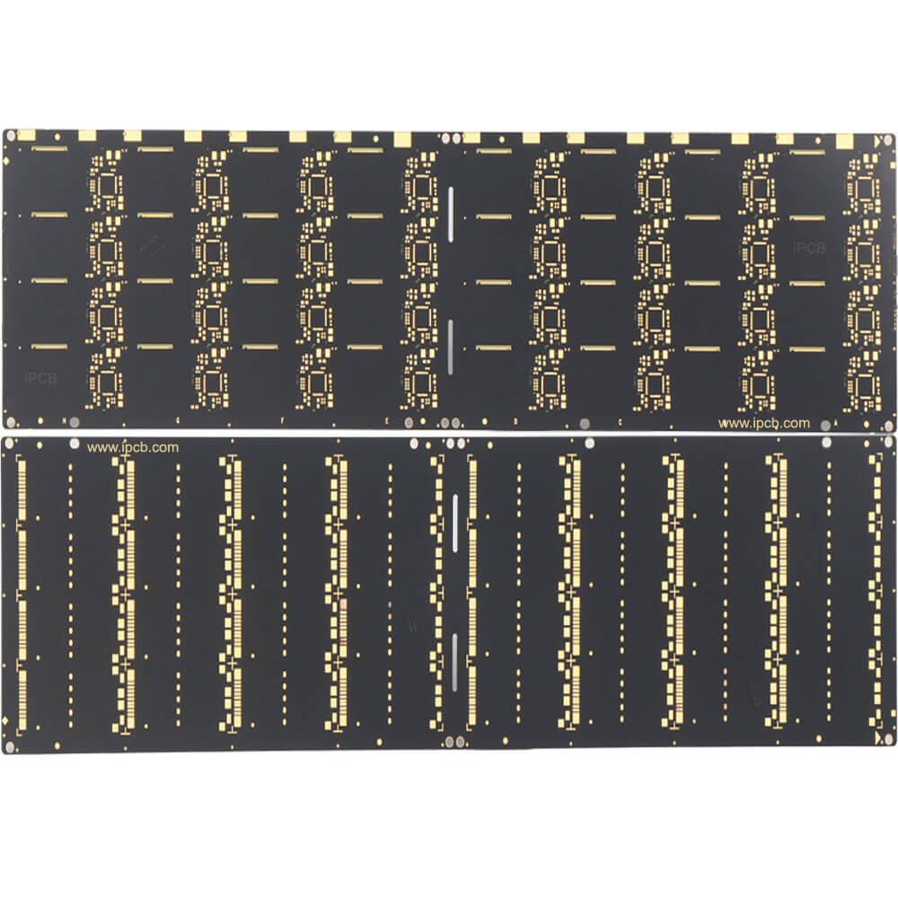
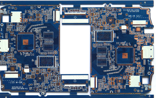
IC packaging board refers to the process of processing the measured wafer according to the product model and function requirements to obtain independent chips. IC packages primarily provide a medium to connect fine silicon chips to widely-spaced printed circuit boards and protect the devices from moisture.
Specific packaging forms include:

packaging form
Lead package

In the late 1970s, the first package to be widely accepted on the market was dual-in-line (DIP), a ceramic and plastic package. The leads are drawn from both sides of the package and are perpendicular to the package. The package can be mounted on the PCB by inserting the pin into the through hole in the board, then clipping the lead to the other side of the board and soldering it using wave soldering technology. The package can accommodate a maximum number of leads of 40 and a 0.65mm plate spacing.
In the late 1970s and early 1980s, surface mount appeared. The leads (pins) and components on the chip are welded to a surface of the circuit board rather than through it. This allows both sides of the board to be used to bond the chip, using reflow soldering technology during installation, with a maximum pin count of 80.
By the mid-1980s, packages with leads on all sides appeared. This package is called quad flat package (QFP) (the lead is shaped like a seagull wing) or lead chip carrier (the lead is bent). J). The most commonly used typical quadrangle flat package has a pitch of 0.65mm or 0.5mm and a lead count of up to 208. These packages were widely used in the hard disk drive and graphics markets in the early 1990s.
In the late 1980s and early 1990s, the exposed-Pad Leaded Package was born. The package is a quadrangle flat or smaller shape package with the chip bonding end exposed at the bottom. These exposed bonding ends can be welded to the circuit board, establishing an efficient heat dissipation path for the chip.
The miniature Lead Frame (MLF) family of packages was developed in the 1990s. MLF is close to the Chip Scale Package (CSP), the bottom lead end of the Package is used to provide electrical contact with the PCB board, as opposed to the Gull wing lead Soic and Qual Package, so this Package helps ensure heat dissipation and electrical performance.
2. Layered packaging

layered packaging
In the 1990s, a new type of packaging, called ball Grid Array (BGA), emerged using layered plates as substrate materials. Lead frame-based packaging can only lead to the periphery of the packaging... The leads of the ball grid array package can be guided to the solder ball at the bottom of the entire package. Initially, the typical ball pitch for BGA package boards was 1.27 mm.
3. Wafer level packaging

wafer level packaging
When space is required, the best packaging is no packaging at all. Additional processing can be done at the wafer level to produce devices that can be installed directly on the circuit board. This process typically involves using a redistribution layer to transfer the fine spacing on the wafer to the coarser spacing (typically 0.5mm) on the chip itself, and then creating bump points on the function of the rearrangement. The core will be separated separately, and the wafer level package is the convex block core.
4. System-level encapsulation (SIP)

Now a new round of integration is putting multiple chips in a package called system-level package (SIP). Multi-chip packaging can be achieved by placing two or more chips in the same package (usually using layered substrates), or by stacking one chip on top of another in the same package.
5. Development of packaging interconnect technology

Interconnect describes how chips are connected to a packaged substrate. In most packages, the package body is first joined to the front surface of the chip connection terminal on the substrate (lead frame or layering), and then the chip pad is joined to the lead finger of the substrate using gold or aluminum wire. The superior. This interconnect technique is called lead bonding and is suitable for most packaging applications. A new interconnection scheme is called Flip Chip Bonding. A conductive bump is generated on the chip surface at the pad position. The bump chip is then flipped and connected directly to the substrate. In most cases, a layered substrate is used. Ball adhesion will use reflow soldering process. After connecting the substrate and reflow, a bottom-fill process is used between the chip and the substrate to reduce stress caused by the welding part of the device during use.
6.Packaging Materials Plastic packaging is liable to damp and moisture. The initial package was a through-hole installation, which required less reliability because the heat generated during welding was far from the package (on the other side of the board). The industry has been working to improve mold combinations and chip connection materials to eliminate the need for dry assembly. Another recent requirement for packaging materials is to be completely lead-free and to use "green materials" that meet environmental requirements.
7, packaging process on the wafer process of wafer after scribing process was cut ChengXiaoJing round (Die), and then cut the wafer stick on the substrate (lead frame) corresponding island of framework, then use superfine with metal (gold, tin, copper, aluminum) or between a conductive resin chip bonding pad and IC package substrate corresponding lead connection, form the circuit; The individual chips are then encapsulated and protected by a plastic case. After plastic packaging, it is necessary to carry out a series of operations such as post-mold curing, trimming molding, electroplating and printing. After the packaging is completed, the finished product is tested, usually through incoming materials, testing, packaging, and finally warehousing and shipment. Typical packaging process: cutting, loading, bonding, plastic packaging, deburring, electroplating, printing, cutting ribs and forming, appearance inspection, finished product testing, packaging and delivery.