Abstract: There are many packaging types for semiconductor device s, from DIP, SOP, QFP, PGA, BGA to CSP to SIP. The technical indicators are more advanced from generation to generation. These are all developed by the predecessors based on the assembly technology and market demand at that time. Generally speaking, it has about three major innovations: the first time was from pin plug-in packaging to surface-mount packaging in the 1980s, which greatly increased the assembly density of printed circuit boards; the second time was in In the 1990s, the advent of the ball moment positive package not only met the market’s demand for high pins, but also greatly improved the performance of semiconductor devices; wafer-level packaging, system packaging, and chip-level packaging are now the third innovations The product, its purpose is to minimize the packaging. Each type of packaging has its unique aspects, namely its advantages and disadvantages, and the packaging materials, packaging equipment, and packaging technology used vary according to its needs. The driving force driving the continuous development of semiconductor packaging is its price and performance.
1 Overview of semiconductor device packaging
Electronic products are composed of semiconductor devices (integrated circuits and discrete devices), printed circuit boards, wires, complete machine frames, casings, and displays. The integrated circuits are used to process and control signals. Discrete devices are usually signal amplification and printing. PCB circuit boards and wires are used to connect signals, the frame shell of the whole machine is used for support and protection, and the display part is used as an interface for communication with people. Therefore, semiconductor devices are the main and important part of electronic products, and have the reputation of "industrial rice" in the electronics industry.
my country developed and produced its first computer in the 1960s. It occupies an area of about 100 m2 or more. Today's portable computers are only the size of a schoolbag, while future computers may only be the size of a pen or smaller. This rapid reduction in the size of computers and their increasingly powerful functions are a good evidence of the development of semiconductor technology. The credit is mainly due to: (1) The substantial increase in semiconductor chip integration and wafer fabrication (Wafer fabrication) The improvement of the lithography accuracy has made the chip more powerful and the size has become smaller; (2) The improvement of semiconductor packaging technology has greatly increased the density of integrated circuits on the PCB printed circuit board, and the volume of electronic products has been greatly increased. To lower.
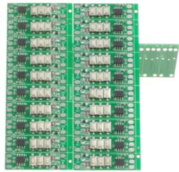
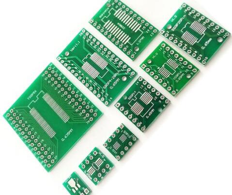
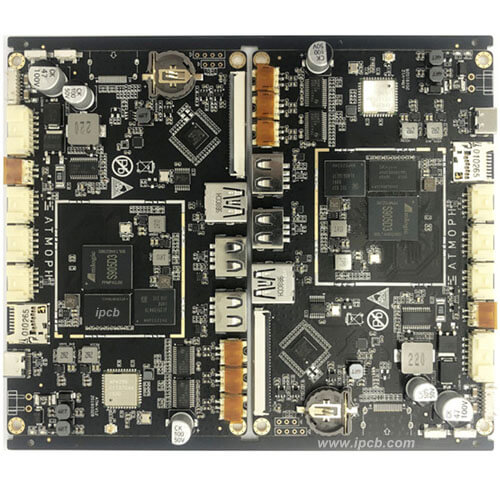
The improvement of semiconductor assembly technology (Assembly technology) is mainly reflected in the continuous development of its package type (Package). Generally referred to as assembly (Assembly) can be defined as: the use of film technology and micro-connection technology to connect the semiconductor chip (Chip) and the frame (Leadframe) or substrate (Sulbstrate) or plastic sheet (Film) or the conductor part of the printed circuit board In order to lead out the wiring pins, and fix them by potting and sealing with a plastic insulating medium, forming the process technology of the overall three-dimensional structure. It has the functions of circuit connection, physical support and protection, external field shielding, stress buffering, heat dissipation, oversize and standardization. From the plug-in package in the triode era and the surface mount package in the 1980s to the current module package, system package, etc., predecessors have developed many package forms, and every new package form may require New materials, new processes or new equipment are used.
The driving force driving the continuous development of semiconductor packaging is its price and performance. The end customers of the electronic market can be divided into three categories: home users, industrial users and national users. The biggest feature of home users is that the price is cheap and the performance requirements are not high; national users require high performance and the price is usually tens or even thousands of times that of ordinary users, mainly used in military and aerospace, etc.; industrial users are usually price and performance All fall in between the above two. Low prices require cost reduction on the original basis, so that the less materials used, the better, and the larger the one-time output, the better. High performance requires a long product life and can withstand harsh environments such as high and low temperatures and high humidity. Semiconductor manufacturers are always trying to reduce costs and improve performance. Of course, there are other factors such as environmental protection requirements and patent issues that force them to change packaging types.
2 The role of encapsulation
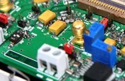
Package (Package) is necessary for the chip, but also very important. Packaging can also be said to refer to the housing used to install the semiconductor integrated circuit chip. It not only protects the chip and enhances the thermal conductivity, but also serves as a bridge between the internal world of the chip and the external circuit and the general function of specifications. The main functions of encapsulation are:
(1) Physical protection. Because the chip must be isolated from the outside world to prevent the impurity in the air from corroding the chip circuit and cause the electrical performance to decline, protect the chip surface and connecting leads, etc., so that the fairly soft chip is protected from external force damage and external damage in terms of electrical or thermal physics. Environmental impact; at the same time, the thermal expansion coefficient of the chip is matched with the thermal expansion coefficient of the frame or substrate through packaging, which can relieve the stress caused by changes in the external environment such as heat and the stress caused by the heat of the chip, thereby preventing the chip Damage failure. Based on the requirements of heat dissipation, the thinner the package is, the better. When the power consumption of the chip is greater than 2W, a heat sink or heat sink needs to be added to the package to enhance its heat dissipation and cooling function; when 5 to 1OW, forced cooling must be adopted. On the other hand, the packaged chip is also easier to install and transport.

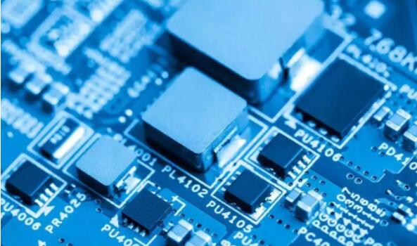
(2) Electrical connection. The size adjustment (pitch conversion) function of the package can be adjusted from the extremely fine lead pitch of the chip to the size and pitch of the mounting substrate, thereby facilitating the mounting operation. For example, from chips with sub-micron (currently below 0.13μm) as the feature size, to chip solder joints with 10μm as the unit, to external pins with 100μm as the unit, and finally printed in millimeters. Circuit boards are all realized by packaging meters. The packaging here plays a role of transforming from small to large, from difficult to easy, from complex to simple, which can reduce operating costs and material costs, and improve work efficiency and reliability, especially by realizing wiring length and impedance The ratio is as low as possible to reduce the connection resistance, parasitic capacitance and inductance to ensure the correct signal waveform and transmission speed.
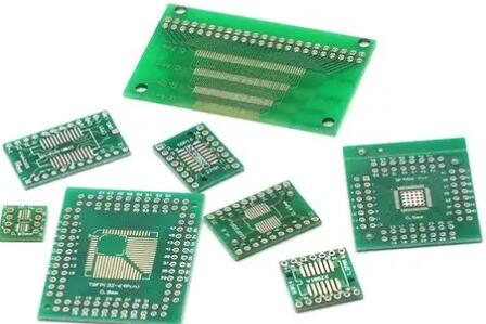
(3) Standardization. The general function of specifications means that there are standard specifications for the size, shape, number of pins, spacing, length, etc. of the package, which is easy to process and easy to match with the printed circuit board. The related production lines and production equipment are universal. This is very convenient for packaging users, circuit board manufacturers, and semiconductor manufacturers, and it is easy to standardize. In contrast, bare chip mounting and flip-chip mounting currently do not have this advantage. Since the quality of assembly technology also directly affects the performance of the chip itself and the design and manufacturing of the printed circuit board (PCB) connected to it, for many integrated circuit products, assembly technology is a very critical part.
3 Package classification
The packaging of semiconductors (including integrated circuits and discrete devices) has undergone several generations of changes, from DIP, SOP, QFP, PGA, BGA to MCP and then to SIP. The technical indicators are advanced from generation to generation, including chip area and packaging area. The ratio is getting closer and closer to 1, the applicable frequency is getting higher and higher, the temperature resistance is getting better and better, the number of pins is increased, the pin spacing is reduced, the weight is reduced, the reliability is improved, and the use is more convenient. There are many types of packages, and each type of package has its own unique features, namely its advantages and disadvantages. Of course, the packaging materials, packaging equipment, and packaging technology used vary according to its needs.