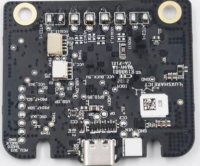
The glue for the PCB circuit board to seal the IC chip is a colorless, transparent and environmentally friendly UV glue used for bonding the IC chip and the FPC flexible circuit board. The UV glue is irradiated by ultraviolet light and does not require heating to effectively protect the quality of the IC chip. Ultraviolet uv glue improves the bonding ability of the contact part between the chip and the fpc by sealing and protecting the ic chip, so that the ic chip has a long-term safe use environment. The uv glue is insulating, waterproof and moisture-proof.
The IC package ultraviolet light curing uv adhesive has the following performance characteristics: 1 good moisture resistance 2 flexibility, energy consumption, and a certain cushioning effect 3 strong bonding performance, not easy to drop parts 4 curing process does not require heating and will not cause damage to the ic chip 5 Non-corrosive ic chip UV glue usage method: 1. Clean the electronic components to be packaged. 2. Use a dispenser to apply the glue on the surface of the electronic component to be packaged, let it flow naturally, and make sure that there are no bubbles. 3. Irradiate the UV lamp until the glue is fully cured (the irradiation time depends on the type, power, and irradiation distance of the UV lamp) ipcb is happy to answer for you:
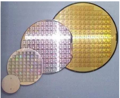
The connection lines between the billions of transistors in the chip and the connection lines with other components, such as the connection lines of the body resistor, the junction capacitor connection line, and the welding area of the external lead wire, are all successfully manufactured at the same time. The conductor material used is gold.

The method of making these connecting wires is,
1. Through photolithography and etching (the etching solution is usually hydrofluoric acid that can corrode silicon dioxide or silicon nitride), the entire surface of the passivated chip is opened at both ends of each connecting line.
2. Plasma sputtering coating method is used to coat a copper film with a thickness of about 1 micron on the entire chip surface where the window is opened. This copper film is not used as a connecting wire, but for making the connecting wire "as a wedding dress", please continue to look down.
3. Using the method of photolithography and etching, a window is opened on the complete copper film where it will be used to make the connection line and the welding area in the future. This kind of copper film that opens the window is similar to a mask for printing patterns or words on a t-shirt, etc.; but it is different from that kind of mask. Because that type of mask can be put on and removed multiple times and reused; the copper mask made this time is fixed and used once. Therefore, this type of mask is called a "dead mask." The corrosive liquid used to corrode the copper film this time is different from the corrosive liquid used to corrode the passivation layer in the previous process It generally uses a ferric chloride solution that can corrode copper.
4. On the copper dead mask, a gold film with a thickness of about 1 micron, which is used as a conductor, is plated by a vacuum evaporation coating method.
5. Reuse the etching method used in the previous process (No photolithography is needed this time), remove the copper dead mask (also remove the gold film that exists on the surface of the dead mask), and the remainder The gold film is the welding area between the transistors and the connection lines and the external lead wires needed by the chip.