This paper will introduce some of the daily common IC Substrate packaging principle and functional characteristics, through understanding the packaging of various types of IC, electronic engineers in the design of electronic circuit principle, can accurately choose IC, and for the factory mass production of burning, can quickly find the corresponding IC packaging burning block model.
1. DIP dual in-line package
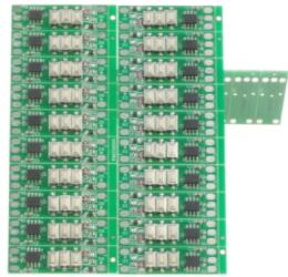
It refers to the integrated circuit chip packaged in the form of dual in-line. Most small and medium scale integrated circuits (ics) are packaged in this form, and the number of pins generally does not exceed 100. An IC in a DIP package has two rows of pins that need to be plugged into a socket on a DIP chip. Of course, it can also be directly inserted into the circuit board with the same number of holes and geometric arrangement for welding. Dip-packaged chips should be removed with care from the chip socket to avoid damage to the pins. Packaging has the following characteristics: Suitable for PCB(printed circuit board) perforation welding, easy to operate.The ratio between chip area and package area is large, so the volume is also large. It is a popular plug type package, application range includes standard logic IC, memory and microcomputer circuit, etc.

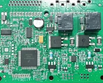
2. QFP/ PFP type encapsulation
The distance between the pins of the chip package is very small, the pin is very thin, the general large-scale or ultra large integrated circuit adopts this kind of package form. Chips packaged in this form must be welded to the motherboard using SMD (Surface mount device technology). SMD installed chips do not need to punch holes in the motherboard, generally on the motherboard surface has a good design of the corresponding pin solder spot. The chip pin is aligned with the corresponding solder joint, and the main board can be welded.
Packaging has the following characteristics: Suitable for SMD surface mounting technology to install wiring on PCB board; Low cost, suitable for medium and low power consumption, suitable for high-frequency use; Easy to operate, high reliability; The ratio between chip area and package area is small; Mature sealing type, can use the traditional processing method. At present, QFP/PFP package is widely used, and A chip of many MCU manufacturers adopts this package.
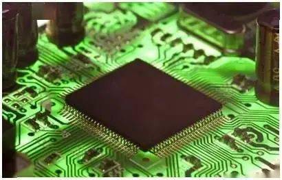
3. BGA type encapsulation
With the development of IC technology, the requirements of IC packaging are more stringent. This is because the packaging technology is related to the functionality of the product. When the frequency of IC exceeds 100MHZ, the traditional packaging method may produce the so-called "CrossTalk" phenomenon, and when the Pin number of IC is greater than 208 Pin, the traditional packaging method has its difficulty. Therefore, in addition to the USE of QFP packaging, most of the current high pin number chips are switched to BGA(BALL Grid Array PACKAGE) packaging technology. Packaging has the following characteristics: Although the number of pins increases, the distance between pins is much larger than that of QFP encapsulation, which improves the yield of finished product.
The contact surface between the array solder ball and the substrate is large and short, which is conducive to heat dissipation; The pin of the array solder ball is very short, which shortens the transmission path of the signal and reduces the inductance and resistance of the lead. The signal transmission delay is small and the adaptive frequency is greatly increased, so the circuit performance can be improved. Assembly can be coplanar welding, reliability greatly improved; Suitable for MCM packaging, can achieve high density and high performance of MCM.
4. SO type packaging
Type package includes :SOP(small shape package), TOSP (thin small shape package), SSOP (reduced type SOP), VSOP (very small shape package), SOIC (small shape integrated circuit package) and other similar to the QFP form of package, but only on both sides of the pin chip package form, This type of package is one of the surface mount type packages, and the pins lead out from both sides of the package in an "L" shape. The typical characteristics of this type of packaging is to make a lot of pins around the packaging chip, packaging operation is convenient, high reliability, is one of the mainstream packaging methods, currently more common is applied to some memory types of IC.
5. QFN package type
Is a leadless square flat package that is lead-free with peripheral terminal pads and a chip pad for mechanical and thermal integrity exposure. The package can be square or rectangular. The four sides of the package are equipped with electrode contacts. Due to the absence of pins, the mount occupies a smaller area and a lower height than QFP.
Packaging features:
Surface mount package, no pin design; The pin less pad design occupies a smaller PCB area; Components are very thin (< 1mm), which can meet the application with strict requirements on space; Very low impedance, self-induction, can meet high speed or microwave applications; It has excellent thermal performance, mainly because there is a large area of heat dissipation pad at the bottom; Lightweight for portable applications. The small form factor of the package can be used in portable consumer electronics such as notebook computers, digital cameras, personal digital assistants (PDAs), mobile phones and MP3 players. From the perspective of the market, QFN packaging is attracting more and more attention from users. Considering the cost and volume factors, QFN packaging will be a growth point in the next few years, and the development prospect is extremely optimistic.
6. PLCC package type
It is a plastic chip packaging carrier with lead. The surface mount package, with the pins leading from the four sides of the package, forms a "D" shape and is much smaller than the DIP package. The package is suitable for PCB mounting and wiring with SMT surface mounting technology, and has the advantages of small size and high reliability. For special pin chip package, it is a kind of patch package, the pin of this package is bent inward at the bottom of the chip, so the chip pin is not visible in the top view of the chip. The welding of this chip adopts reflow welding process, which requires special welding equipment. It is also very troublesome to take off the chip during debugging, and it is rarely used now.