What is the thermal design inPCB processing? From what aspects do we need to understand this problem? The scope of application of thermocouple temperature measurement is very wide, and the problems encountered are also diverse. Therefore, this chapter can only cover some important aspects of thermocouple temperature measurement. Thermocouple is still one of the main methods of temperature measurement in many industries, especially in steelmaking and petrochemical industries. However, with the advancement of electronics, resistance thermometers have become more and more widely used in industry, and thermocouples are no longer the only and most important industrial thermometers.
The practical application of thermoelectric phenomena is of course the use of thermocouples to measure temperature. The complex relationship between electron energy and scattering makes the thermoelectric potentials of different metals different from each other. Since the thermocouple is such a device, the difference in thermoelectric potential between its two electrodes is an indication of the temperature difference between the hot and cold ends of the thermocouple. If the thermoelectric potential of all metals and alloys are different, it is impossible to use Thermocouple to measure temperature.
1: Create packages that are not in the package library. Before designing the PCB board diagram, if a component in the schematic diagram cannot find the package model in the package library, you need to use the component package model editor to create a new one. Make sure that the package model of the used component is in the package library ( Can be multiple library files) is complete
2: Set the PCB board drawing design parameters. According to the needs of the circuit system design, set the number of layers, size, color, etc. of the PCB board.

3: Load the network table. Load the netlist generated by the schematic, and automatically load the component package model into the PCB design window.
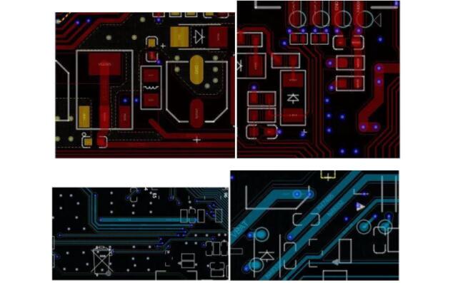
4: Layout. The method of combining automatic layout and manual layout can be used to place the component packaging model in an appropriate position within the PCB planning range, that is, to make the component layout neat, beautiful, and conducive to wiring.
5: Wiring. Set the wiring design rules and start automatic wiring. If the wiring is not completely successful, manual adjustments can be made.
6: Design rule check. Carry out design planning check on the designed PCB board (check whether the components overlap, whether the network is short-circuited, etc.), if there are errors, modify them according to the error report.
7: Simulation analysis of PCB board proofing. Carry on simulation analysis to the signal processing of PCB board, mainly analyze the influence of layout and wiring on various parameters, so as to improve and modify.
8: Save the output. The designed PCB diagram can be saved, printed in layers, and output PCB design files.
Note: Before designing the PCB board drawing, if a component in the schematic diagram cannot find the package model in the package library, you need to use the component package model editor to create a new one. It is necessary to ensure that the package model of the component used is in the package The library (can be multiple library files) is complete to ensure the smooth progress of the PCB design.