IC PCB & Packaging- When talking about the future of wearable technology, the future course of wearable technology innovation is clear. It's loud and clear that to succeed, wearable electronics must be small and still perform. This article focuses on the requirements for wafer - level chip - level packaging in SRAM .
To reduce footprint, and thus overall board space, microcontrollers migrate to smaller process nodes every other generation. At the same time, they are evolving to perform more complex and powerful operations. As operations become more complex, there is an urgent need to increase caching. Unfortunately, with each new process node, adding embedded cache (embedded SRAM) becomes challenging for a number of reasons, including higher SER, lower yield, and higher power consumption. Customers also have custom SRAM requirements. For MCU manufacturers to provide all possible cache sizes would require them to have a product portfolio that is too large to manage. This has driven the need to limit the embedded SRAM on the controller core and to cache it via an external SRAM.
However, since external SRAM takes up a large amount of PCB board space, using external SRAM faces the challenge of miniaturization. Due to its six-transistor architecture, reducing the size of the external SRAM by porting the external SRAM to a smaller process node will introduce the same problems that have plagued the miniaturized embedded SRAM.
This brings us to the next alternative to this age-old problem: reducing the ratio of chip packaging to chip size in the external SRAM. Typically, packaged SRAM chips are many times the size of the bare chip (up to 10 times). A common solution to this problem is to not use encapsulated SRAM chips at all. It makes sense to take an SRAM chip (1/10 size) and then package it with an MCU chip using complex multi-chip packaging (MCP) or 3D packaging technology (also known as SIP system-level packaging). But this approach requires significant investment and is only feasible for the largest manufacturers. From a design perspective, this also reduces flexibility because components in SIP are not easily replaced. For example, if the new technology SRAM is available, we cannot easily replace the SRAM chip in SIP. To replace any of the bare chips in the package, the entire SIP must be re-authenticated. Requalification requires reinvestment and more time.
So is there a way to save board space while excluding the SRAM from the MCU without putting the MCP in trouble? Going back to the core-to-chip size ratio, we do see room for significant improvement. Why don't you check if there's a package that fits tight to the mold? In other words, if you cannot unpack, please reduce the size scale.
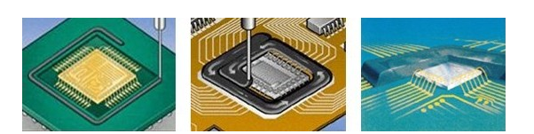
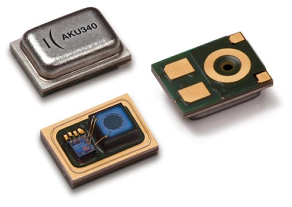
Currently the most advanced approach is to reduce the size of the chip package by using WLCSP (wafer level chip level package). WLCSP refers to the technology of cutting individual units from a wafer into small pieces and then assembling them in a package. The device is essentially a bare chip with a raised dot or spherical array pattern that does not require any bonding lines or intermediate layer connections. Depending on the specifications, the area of a chip-level package is up to 20% larger than that of the chip. The process has now reached an innovative level where manufacturing plants can produce CSP components without increasing the chip area (with only a slight increase in thickness to fit the bump/sphere).
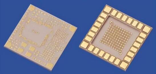
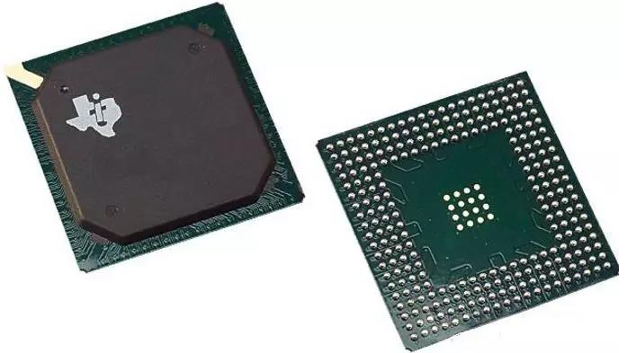
Numbers. Wafer - on - chip packaging (WLCSP) provides the most advanced method for reducing the size of the packaged bare - chip. The WLCSP shown here was developed by DECA Technologies and does not increase the area of the chips that make up it. (Credit: DECA Technologies/ Cypress Semiconductor)
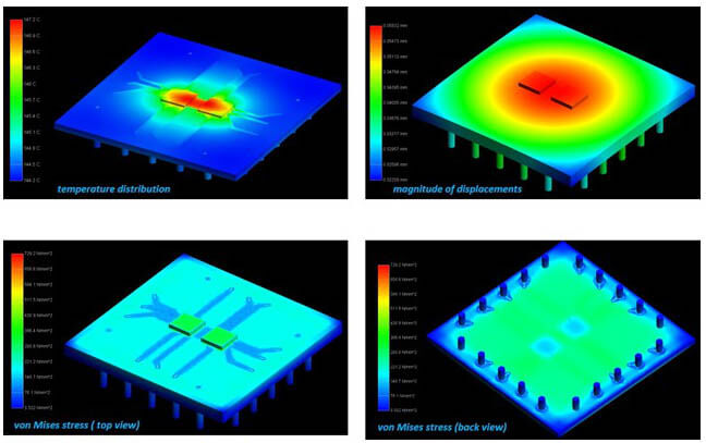
CSP has some advantages over uncoated film. CSP devices are easier to test, handle, assemble, and rewrite. They also have enhanced thermal conductivity properties. When the core is transferred to newer process nodes, it is possible to reduce the core while standardizing the CSP size. This ensures that CSP components can be replaced by a new generation of CSP components without any complications associated with changing the mold.
Obviously, these space savings are important in terms of the demand for wearables and portable electronics. For example, the 48-ball BGA used in the IC memory in many wearable devices today has a size of 8mmx6mmx1mm (48mm3). By comparison, the same part in a CSP package measures 3.7mmx3.8mmx0.5mm (7mm3). In other words, you can reduce the volume by 85%. This savings can be used to reduce PCB area and thickness for portable devices. As a result, the demand for WLCSP based devices from wearables and Internet of Things (IoT) manufacturers is not limited to SRAM, but there is a new demand.