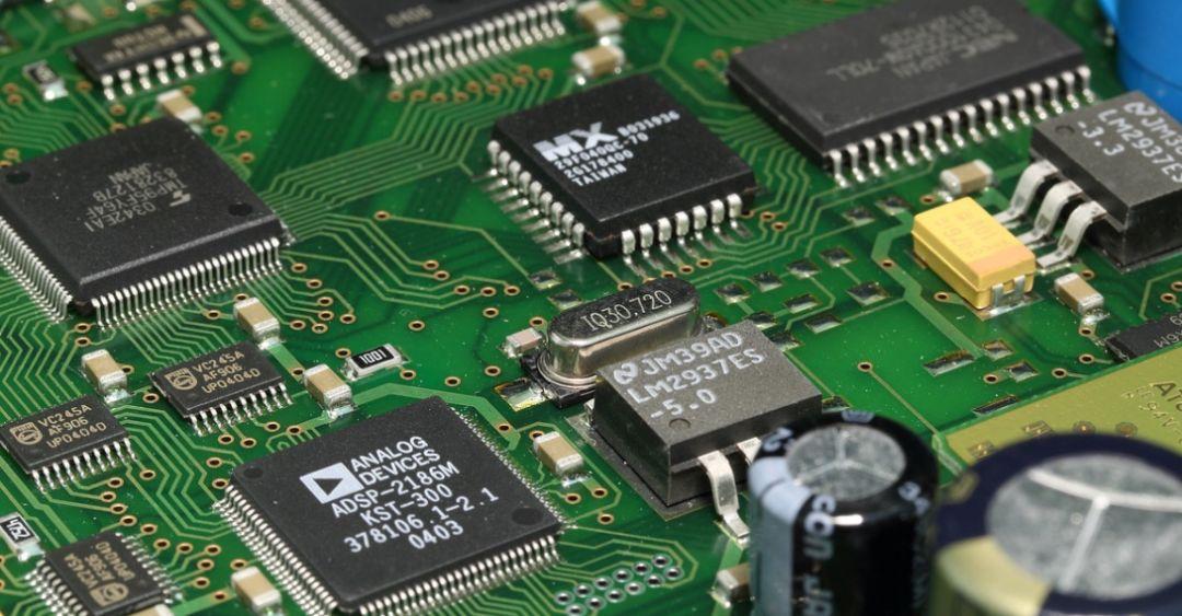
The technique of cutting individual units from wafers and then packaging them has long been the norm for packaging semiconductor integrated circuits for decades. However, this approach is not currently being adopted by major semiconductor manufacturers due to high manufacturing costs and the increasing RF component of today's modules. Thus, the emergence of wafer-level packaging (WLP) has led to a paradigm shift in the development of low-cost packaging. WLP is a wafer level packaging technology prior to the cutting of wafer packaging devices.
Using standard tools and processes, WLP acts as an extension of the wafer manufacturing process. Eventually, the manufactured WLP DIE will have a metalized pad on the surface of the chip and a solder dot deposited on each pad prior to cutting the wafer. This, in turn, makes WLP compatible with traditional PCB assembly processes and allows device testing on the wafer itself. As a result, it is a relatively low cost and efficient process, especially as the wafer size increases and the chip DIE shrinks. The size of wafers has been increasing over the past few decades, from 4, 6, and 8 inches in diameter to 12 inches. This results in an increase in the number of DIEs per wafer, which lowers manufacturing costs. In terms of electrical performance, WLP is superior to other packaging technologies, in the sense that once a WLP device is integrated into a dense RF module, it results in a significant reduction in EM parasitic coupling because the interconnection between the device and the PCB is relatively short, unlike the wire-bonded interconnection used in some types of CSP technologies.
WLP chip flip-chip technology
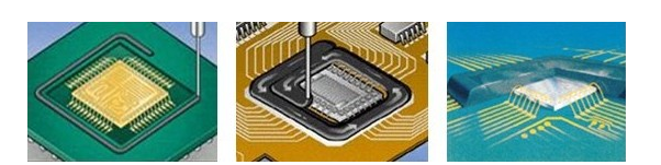
Flip-chip technology, also known as the Controlled Collapse Chip Connection (C4), is one of several chip assembly technologies developed by IBM in the 1960s. Although wire bonding based packaging technology is more flexible in terms of free inductive capability for laboratory debugging after the hardware is built, and also provides good thermal conductivity, the use of solder bulges in flip-chip packaging technology makes the electrical connection between the package substrate and the chip provide relative size reduction, reduced latency, and better isolation in terms of its input and output pins. Figure 1 illustrates the basic structure of the chip DIE on the substrate, with a solder ball at the top of the Cu column growing on the chip surface. The solder joint is usually encapsulated with a filler mold compound to provide mechanical support for the solder joint.

WLP chip level package
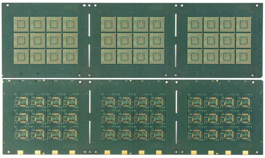
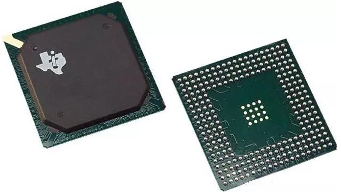
Chip scale packaging (CSP) is one of the most commonly used packaging methods in microelectronics and semiconductor industry. While several types of CSP technologies are already available to microchip manufacturers, new types continue to emerge to meet the demand for products that support new features and new application-specific products. These packaging requirements may vary depending on the required level of reliability, cost, additional features, and overall size. As the name implies, the package size of the CSP is roughly the same as the chip DIE size, which is one of its main advantages. By adopting the WLP manufacturing process, CSP is constantly being developed to achieve the smallest possible package-die size ratio. As shown in Figure 2, the ball grid array (BGA) style of CSP in the package allows for several interconnections while simplifying PCB wiring, increasing PCB assembly throughput and reducing manufacturing costs.
")
Other encapsulation technologies
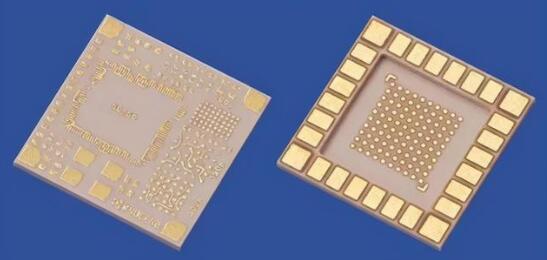
There are several other forms of integrated IC packaging that allow seamless integration into application-customized module packages. Quad Flat Package (QFP) is one of the earliest surface-mount IC package technologies,where the structure of the package is composed of four sides with extended interconnect leads, as shown in Figure 3(a). The raised leads are connected to the package frame to form a metal-insulator-metal (MIM) type capacitor between the leads and the chip DIE metal, which can be used as a matching element. This technique is suitable for millimeter sized ICs where the number of peripheral pins in the package can reach more than 100 pins. There are several derivatives of this type of encapsulation, depending on the material used, such as ceramic quad flat pack, thin quad flat pack, plastic quad flat pack, Plastic Quad Flat Pack) and Metal Quad Flat Pack (MQFP). The QFN, Quad Flat No Lead, shown in Fig. 3(b) is one of several surface-mounted packaging technologies formed from a flat copper lead frame and a plastic package used as a heat transfer pad for the radiator. Wire bonding can also be used for interconnections, and since bond lines are not only conductors but also inductors, they generally affect the performance of devices under this encapsulation technique, unless it is considered as part of the overall design. Although the QFN is an interconnect consisting of four sides, the bi-plane unled leads (DFN) have also appeared and form both sides of the interconnect plane leads.