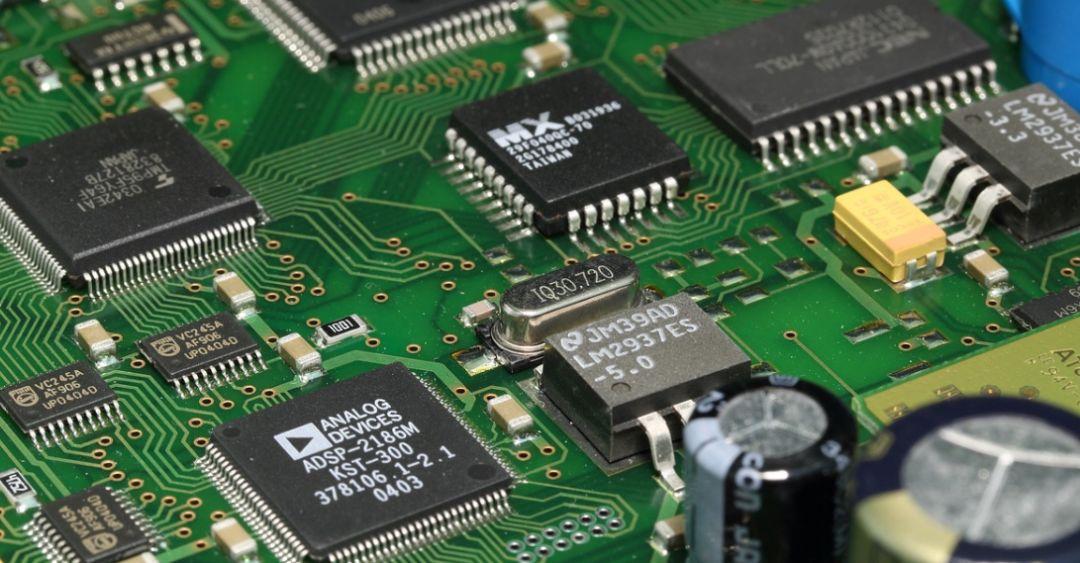
MEMS device is small in size and low in cost, which is the development direction of future sensors. With the progress of MEMS IC packaging technology, inertial MEMS IC packaging sensor and medium angular frequency sensor are inertial components with high resolution and low cost, which are used to measure the yaw Angle and rotation roll rate of missile attitude. In MEMS devices, the packaging technology is very important. In addition to the integration technology, the packaging has become another core of the durable inertial MEMS devices. We discuss and study the packaging technology, in order to improve the reliability of MEMS devices.
1. summary of MEMS IC packaging
MEMS, also known as MEMS, is a relatively independent intelligent system with a very small size, only a few millimeters or even smaller. It is composed of three major parts: sensors, actuators and micro-energy. MEMS design includes many disciplines, including physics, chemistry, material engineering, electronic engineering and a series of disciplines. MEMS system is applied in many fields, among which automotive electronics, computer, consumer electronics and network communication are the most common four fields. MEMS process has many similarities with traditional IC process. MEMS uses IC process for reference, such as lithography, film deposition, doping, etching, chemical mechanical polishing, etc. For millimeter or nanometer level processing technology, traditional IC process cannot be realized. It must rely on micro-processing to carry out fine processing. To achieve the desired structure and function. Micromachining technology includes bulk micromachining technology and surface micromachining technology of silicon. The bulk machining technology is a process of etching silicon substrate along the thickness of silicon substrate, which is an important method to realize three-dimensional structure. Surface micromachining is a process of thin film deposition, lithography and etching. By depositing the structure layer on the sacrificial layer, and then removing the sacrificial layer to release the structure layer, the movable structure is realized.

2. Advantages of MEMS device IC packaging
MEMS is based on the integration of functions on the chip, the size is generally below millimeter, the production process is more precise, requires higher technology, MEMS system has been used as early as abroad, China started late, in MEMS investment gradually increased, the market share is growing. The emergence and development of MEMS is the result of modern scientific innovation, and it is also the evolution and revolution of micro-scale manufacturing technology. MEMS is most widely used in the field of sensors. Due to its small size, light weight and low cost, MEMS products are widely popular, which makes the demand for small volume and high performance MEMS products in a variety of fields grow rapidly. A large number of MEMS products have been found in consumer electronics, medical treatment and other fields. MEMS has the following five characteristics:
2.1 miniaturization
MEMS devices are generally "small", no matter in size, weight, or in terms of energy consumption, cost belongs to the "micro" series, and high working efficiency, short response time.
2.2 Wide material source, excellent performance
The raw material of most integrated circuits and MEMS is silicon, which can be refined by chemical reactions from silicon dioxide, the main ingredient of sand, and the raw material is everywhere. In addition, silicon is as hard as iron, less dense, similar to aluminum, and highly conductive to heat.
2.3 Batch production
Complete MEMS can be manufactured simultaneously on a single silicon wafer, and large scale production can improve production efficiency and save a lot of cost.
2.4 integrated
A system composed of various sensors or actuators with different functions can form a microactuator array and microsensor array, and can also combine devices with various functions to form a complex microsystem. The combination of microactuators, sensors and microelectronic devices creates MEMS with high reliability and stability.
2.5 Interdisciplinary
MEMS design knowledge is extensive and multidisciplinary knowledge intersects. MEMS technology becomes extremely complex and involves various aspects of knowledge. MEMS devices draw on the development achievements of many modern science and technology.
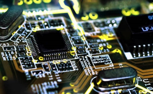
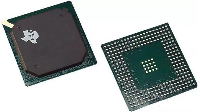
3.MEMS IC packaging device packaging technology
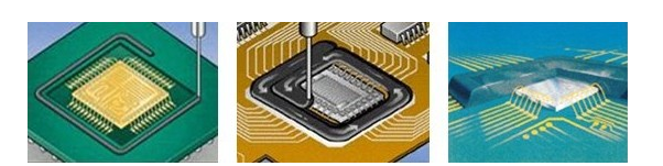
3.1 Reverse assembly welding technology
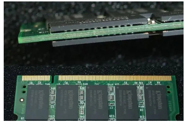
Reverse welding is the face down of the chip, and then packaging with the packaging substrate. The advantage is that the chip is directly connected to the substrate, so the wafer can be directly inverted onto the PCB, and the I/O can be drawn from around the wafer. I/O is directly drawn from the surrounding, and there is no need to connect from an interface, which greatly reduces the length of the interconnection, thus reducing the latency, improving the speed of operation, and achieving the ultimate goal of improving the electrical power. Obviously, for this kind of connection, can maximize the use of space, and will not lead to too much volume because of too many connections, on the contrary, the effect of the flip chip and the original size is almost the same, greatly improving the operating efficiency. In all the surface mount technology, the flip chip can achieve the smallest, the thinest package, so that the whole package after the device size is reduced a lot. Because the bump can fill the entire core, the interconnection density of I/O is also greatly increased, speeding up the efficiency of input and output, and because the connection is shortened, the signal transmission time is shortened, thus greatly improving the electrical performance. For example, in the case of micromicrophones, the lead between the amplifier and the microphone needs to be shortened in order to reduce signal crosstalk and lead inductance. To achieve this, the micromicrophone MEMS chip and the amplifier circuit need to be packaged together. Such device packaging needs to use reverse welding technology, reducing the package size to support a number of other applications. After MEMS device encapsulation, the micromicrophone has the characteristics of low power consumption and high sensitivity, which greatly improves the effect of the microphone. Compared with the traditional electret microphone, the price is much cheaper.
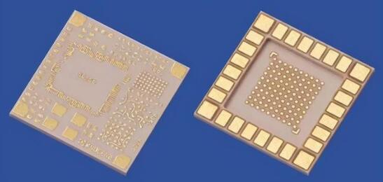
3.2 Multi-chip component technology
Multi-chip components (MCM) are system-level packaging, which is a breakthrough in electronic packaging technology. MCM refers to a package body containing two or more chips connected by the substrate, together constitute the package form of the whole system. It also provides conditions for signal interconnection, I/O management, thermal control, mechanical support and environmental protection for all chips in the module.
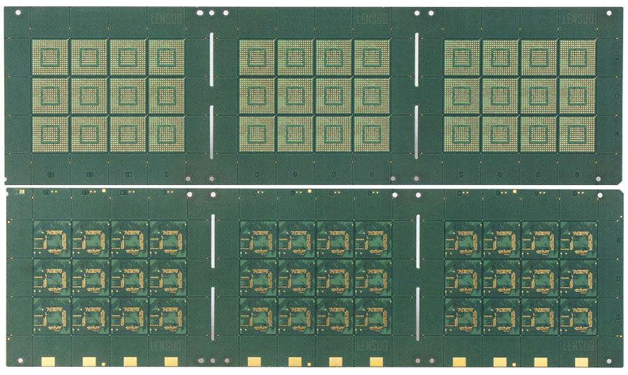
3.3 Multi-chip IC packaging
Multichip packaging is another developing trend of MEMS packaging. Compress the volume of the whole device, adapt to miniaturization, shorten the distance between the signal and the actuator, reduce the influence of the signal and external interference, and put the MEMS chip and the signal processing chip in the same shell. Based on the ceramic substrate, the sensor is installed together with the lead bonding technology, and the substrate is encapsulated. Finally, the MEMS encapsulation is successfully completed.
MCM provides a unique and attractive way to integrate and package MEMS devices that support multiple chip capabilities simultaneously on the same substrate, without changing MEMS and circuit manufacturing technology, and without compromising performance optimization. The MEMS package based on MCM technology can replace the traditional single chip package structure without any problem, but also significantly improve the performance and reliability of the device. For example, the packaging of the acceleration sensor produced by Shanxi Ketai Co., Ltd. is to install the control circuit and MEMS chip on a substrate. Using this packaging technology, the reliability and packaging density of the package are improved in a convenient way, and the production efficiency and the rate of mass production are improved at the same time. From various technical advantages, it is feasible to complete the interconnection between MEMS chip and substrate.
4. Conclusion IC packaging
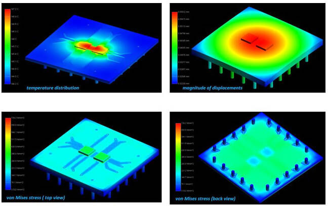
The development of MEMS packaging technology, learning from IC packaging experience, reduce production costs; At the initial stage of chip structure design, the idea of modeling is used to simulate packaging and find suitable materials and processes. With the development of MEMS packaging technology, the process process will only become more and more complex, more and more diversified, accelerate the pace of MEMS packaging technology research, to provide high-quality products.