iPCB.com to explain the chip packaging substrate related packaging process flow:
Packaging substrate or intermediate layer is a very important part of BGA package. Besides for interconnection wiring, it can also be used for impedance control and inductor/resistor/capacitor integration. Therefore, the substrate material is required to have high glass conversion temperature rS(about 175~230 degree Celsius), high dimensional stability, low moisture absorption, and good electrical performance and high reliability. The metal film, insulating layer and substrate medium also have high adhesion performance.
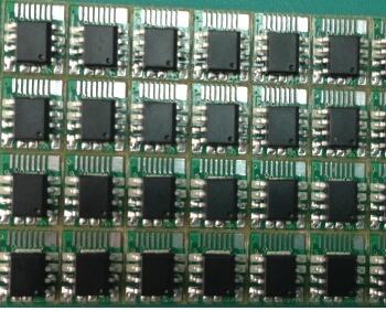
1. Packaging process of line bonded PBGA
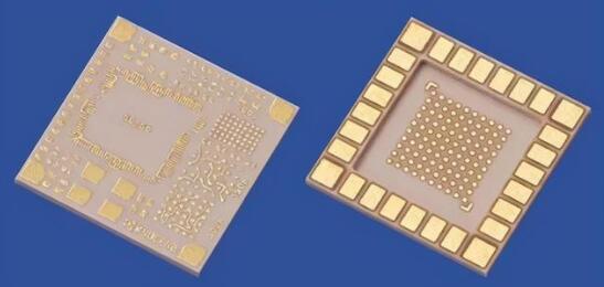
(1) Preparation of BGA substrate
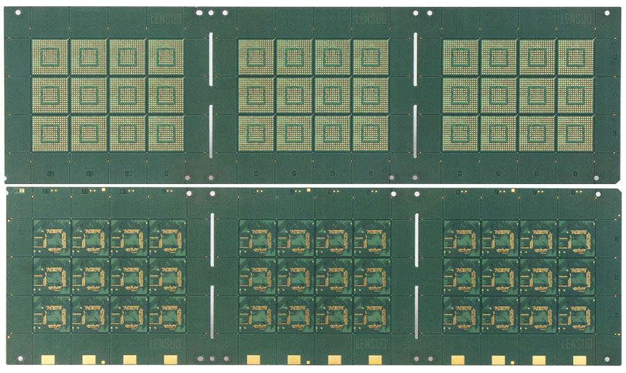
Extremethin (12~18μm thick) copper foil is laminated on both sides of the BT resin/glass core plate, and then metallization is carried out by drilling and through holes. Using a conventional PCB plus 3232 technique, patterns are created on both sides of the substrate, such as guide tape, electrode, and array of solder zones for mounting solder balls. Then add a solder mask and create a pattern that exposes the electrode and solder area. To improve production efficiency, a single substrate usually contains multiple PBG substrates.
(2) Process flow
Wafer thinning to wafer cutting, chip bonding and plasma cleaning - wire bonding - plasma cleaning - molding packaging - assembly solder ball - reflow soldering - surface marking to separation, final inspection and testing bucket packaging chip bonding with silver filling epoxy adhesive to bond on the substrate of IC chips, then the chip and the substrate is realized by using gold wire bonding connection, It is then molded and encapsulated or poured with liquid glue to protect the chip, weld wire and pad. The solder ball 62/36/2Sn/Pb/Ag or 63/37 / Sn/Pb with a diameter of 30mil(0.75mm) with a melting point of 183 degree Celsius is placed on the pad with a specially designed suction tool, and reflow soldering is carried out in a traditional reflow furnace with the maximum processing temperature not exceeding 230 degree Celsius. Substrates are then centrifugally cleaned using a CFC inorganic cleaner to remove the solder and fiber particles remaining on the package, followed by marking, separation, final inspection, testing, and warehousing.

BGA Packaging
2.C-CBGA packaging process
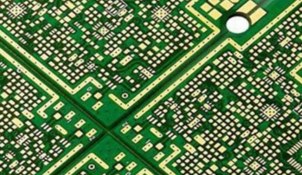
(1) CBGA substrate
FC-CBGA substrate is a multi-layer ceramic substrate, its production is quite difficult. Because the wiring density of the substrate is high, the spacing is narrow, the through hole is many, and the coplanar requirements of the substrate are higher. Its main process is: the first multi-layer ceramic chip high temperature co-firing into multi-layer ceramic metallized substrate, and then on the substrate production of multi-layer metal wiring, and then electroplating. In the assembly of CBGA, the CTE mismatch between substrate, chip and PCB circuit board is the main factor that causes the failure of CBGA products. To improve this situation, in addition to the use of CCGA structure, can also use another ceramic substrate -HITCE ceramic substrate.
(2) Process flow
The preparation of wafer bump groan chip flip and reflow solder -) bottom filling groan thermal grease, distribution of sealing bucket solder ball assembly -) reflow bucket marking + separation groan final inspection bucket test bucket packaging.
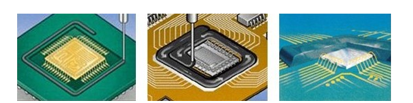
3. Packaging process flow of wire bonded TBGA
(1) BGA carrier
TBGA carriers are usually made of polyimide materials. In the production, the two sides of the carrier belt are copper coated, and then nickel plated and gold plated, and then punched through holes and through holes metallization and graphics are produced. In this lead-bonded TBGA, the heat sink of the package is the addition solid of the package and the core cavity base of the shell. Therefore, a pressure-sensitive binder should be used to bond the carrier tape to the heat sink before packaging.
(2) Packaging process flow
Wafer thinning - wafer cutting - chip bonding - cleaning - lead bonding - plasma cleaning - liquid sealant filling - solder ball assembly - reflow soldering - surface marking - separation - final inspection - test - packaging.