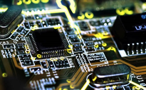
In addition to advanced processes, advanced packaging has become a key technology to continue Moore's Law. Technologies such as 2.5D, 3D and Chiplets have become hot topics in the semiconductor industry in recent years. How, exactly, does advanced packaging play a key role in continuing Moore's Law? What are the characteristics of packaging technologies such as 2.5D, 3D and Chiplets?
Artificial intelligence (AI), Internet of Vehicles, 5G and other applications have emerged, and they all need to use advanced functional chips with high-speed computing, high-speed transmission, low latency and low energy consumption. However, as the demand for computing grows multiple times, how to continue Moore's Law is a challenge for the semiconductor industry.
As chip microscale becomes more difficult, heterogeneous integration is born.
In other words, semiconductor advanced processes are moving into 7 nm, 5 nm, and then 3 nm and 2 nm. Transistor sizes are therefore approaching the physical volume limits of atoms. Electronic and physical limitations also make it more and more difficult for advanced processes to continue to shrink and upgrade.
As a result, in addition to continuing to develop advanced processes, the semiconductor industry is also looking for other ways to keep chips small and efficient. The layout Design of chips then becomes a new solution to continue Moore's Law, and the concept of Heterogeneous Integration Design Architecture System (HIDAS) arises at the historical moment and becomes the innovation momentum of ICchips.
The so-called heterogeneous integration, broadly speaking, is the integration of two different chips, such as memory + logic chip, photoelectric + electronic components, etc., through packaging, 3D stack and other technologies. In other words, the integration of two chips with different processes and different properties can be called heterogeneous integration.
Because the application market is more diversified, the cost, performance and target population of each product are different, so the heterogeneous integration technology required is also different, and the market focus trend gradually emerges. Therefore, IC foundry, manufacturing and semiconductor equipment industry have invested in heterogeneous integration development, 2.5D, 3D packaging, Chiplets and other popular packaging technology, is based on the idea of heterogeneous integration, such as bamboo sprout after a spring spring.
2.5D packaging effectively reduces the cost of chip production
In the past, to integrate chips together, most of the use of System in a Package (SiP) technology, such as PiP (Package in Package) packaging, PoP (Package on Package) packaging. However, as smart phones, AIoT and other applications, not only need higher performance, but also to maintain a small size, low power consumption, in such a case, we must find a way to stack more chips to reduce the volume, therefore, the current packaging technology in addition to the original SiP, but also toward the three-dimensional packaging technology development.
In a nutshell, three-dimensional packaging means using Silicon interposer (Silicon interposer) made directly from Silicon wafers, rather than using the previous plastic "wire carrier", and packaging several chips with different functions directly into a more efficient chip. In other words, adding silicon chips on top of silicon, in a way that increases the cost and physical constraints of the process, keeps Moore's Law alive.
And the stereoscopic package is more familiar with 2.5D and 3D package, here we start from 2.5D package. The so-called 2.5D package, the main concept is to arrange processors, memory or other chips on the Silicon Interposer (Silicon Interposer), which is connected by Micro Bump, so that the metal wires inside the Silicon Interposer can connect the electronic signals of different chips. Then, the TSV is used to connect the lower metal Bump, and the wire carrier plate is used to connect the external metal ball to achieve a closer interconnection between the chip, chip and the packaging substrate.

2.5D and 3D packaging are popular stereo packaging technology. (Source: ANSYS)
The 2.5D packaging technology that is well known at present is nothing more than TSMC's CoWoS. The concept of CoWoS technology is to put semiconductor chips (such as processors, memory, etc.) together on the silicon intermediary layer, and then connect them to the bottom substrate through the packaging process of Chip on Wafer (CoW). In other words, the Chip is first connected to the silicon Wafer through the packaging process of Chip on Wafer (CoW), then the CoW Chip is connected to the substrate and integrated into CoWoS. Using this packaging mode, multiple chips can be packaged together and interconnect through Si Interposer to achieve the effect of small packaging volume, low power consumption and fewer pins.

TSMC CoWos packaging technology concept. (Source: TSMC)
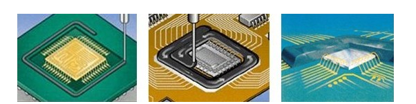
In addition to CoWos, fan-out wafer level packaging can also be classified as a method of 2.5D packaging. The principle of fan-out wafer-level packaging is to pull required circuits from the ends of bare semiconductor to the Redistribution Layer to form packaging. Therefore, there is no need to seal the loading plate, Wire, Bump, which can reduce the production cost by 30%, and also make the chip thinner. At the same time, the chip area can be reduced a lot. It can also replace the higher cost of through silicon perforation, to achieve the goal of integrating different components through packaging technology.
Of course, stereo packaging technology is not only 2.5D, there is ALSO 3D packaging. So, what is the difference between the two, and the SEMICONDUCTOR industry is adopting 3D packaging?
In contrast to the 2.5D package, the 3D package works by creating a transistor (CMOS) structure on the chip and using silicon perforations to connect the electronic signals of different chips above and below, so that the memory or other chips can be directly stacked vertically on

3D packaging is a direct stack of chips. (Source: Intel)
TSMC and Intel actively develop 3D packaging technology
Intel (INTC) and Taiwan Semiconductor (TSMC) have their own technologies for 3D packaging. Intel is using "Foveros" 3D packaging technology, which uses heterogeneous stack logic to handle operations, and can stack each logic chip together. This means, for the first time, extending chip stacking from traditional passive silicon mediators and stacked memory to high-efficiency logic products such as cpus, graphics and AI processors. In the past, stacking was only used for memory, but now heterogeneous stacking is used to enable different combinations of memory and computing chips to be stacked.
In addition, Intel is developing three new technologies, namely co-EMIB, ODI and MDIO. Co-emib can connect with higher computing performance and capability and allow two or more Foveros components to interconnect. Designers can also connect simulators, memory, and other modules at very high bandwidth and very low power consumption. ODI technology provides greater flexibility for the omni-directional interconnection communication between small and medium-sized chips. The top chip can communicate with other small chips like the EMIB technology, and it can communicate vertically with the bottom bare chip below through a silicon through hole (TSV) like the Foveros technology.
Intel Foveros technology concept. (Source: Intel)
The technology also uses large vertical through-holes that supply power directly from the packaging substrate to the top bare plate. These large through-holes are much larger than traditional silicon through-holes and provide a more stable power transmission with lower resistance. And through the stack to achieve higher bandwidth and lower latency. This approach reduces the number of silicon through holes required in the base chip, freeing up more area for the active element and optimizing the bare sheet size.
TSMC, on the other hand, is proposing a "3D multi-chip and system integrated chip" (SoIC) integration solution. The system-integrated on-chip solution combines known good bare crystals of different sizes, process technologies, and materials directly on top of each other.
TSMC notes that the system's integrated chips have several times higher bump density and speed, while significantly reducing power consumption, than traditional 3D integrated circuit solutions that use microbumps. In addition, system-integrated chips are pre-process integrated solutions that connect two or more bare crystals prior to packaging; As a result, the system Integration chipset can leverage the company's InFO or CoWoS back-end advanced packaging technology to further integrate other chips, creating a robust "3D*3D" system-level solution.
In addition, TSMC has launched 3DFabric, which brings together the rapidly growing 3DIC system integration solutions to provide greater flexibility and create powerful systems with robust on-chip interconnection. With different options for front chip stacking and back chip packaging, 3DFabric helps customers connect multiple logic chips together, even tandem high frequency wide memory (HBM) or heterogeneous small chips such as analog, INPUT/output, and rf modules. 3DFabric combines back and front 3D solutions and complements transistor miniatures to continuously improve system performance and functionality, reduce the size and appearance, and speed up product time-to-market.
After introducing 2.5D and 3D, Chiplets is one of the latest advanced packaging technologies to hit the semiconductor industry. Finally, a brief description of Chiplets' features and benefits.
There are three benefits to using Chiplets. Because the cost of advanced process is very high, especially the analog circuit and I / O are becoming more and more difficult to shrink with the process technology. Chips divide the circuit into independent small chips, strengthen their functions, process technology and size, and finally integrate them together to overcome the challenge of process miniaturization. In addition, Chiplets can also use existing mature chips to reduce development and verification costs.
At present, many semiconductor manufacturers have introduced high-performance products in the way of chips. For example, Intel's Intel Stratix 10 GX 10m FPGA is designed with chips to achieve higher component density and capacity. Based on the existing Intel Stratix 10 FPGA architecture and Intel's advanced embedded multi chip interconnect bridging (emib) technology, the product uses emib technology to integrate two high-density Intel Stratix 10 GX FPGA core logic chips and corresponding I / O units. The same is true for AMD's second-generation epyc series processors. Different from the first generation of chip method that combines memory and I / O to form a 14 nm CPU, the second generation is to separate I / O and memory into a chip, and cut the 7 nm CPU into 8 chips for combination.
In a word, in the past, the chip efficiency was improved by the improvement of semiconductor process, but as the component size approached the physical limit, the chip miniaturization became more and more difficult. To maintain the small-size and high-efficiency chip design, the semiconductor industry not only continued to develop advanced processes, but also improved the chip architecture to make the chip from the original single layer, Turn to multi-layer stacking. For this reason, advanced packaging has also become one of the key drivers to improve Moore's law, leading the trend in the semiconductor industry.
The main work of the future intelligent laboratory includes: establishing an AI intelligence system IQ evaluation system and carrying out the world AI IQ evaluation; Carry out the Internet (city) cloud brain research plan, build the Internet (city) cloud brain technology and enterprise map, and serve to improve the intelligence level of enterprises, industries and cities.