IC Chip Design Process
IC Chip design is divided into front-end design and back-end design, front-end design (also known as logical design) and back-end design (also known as physical design) is not unified strict boundaries, involving the design related to the process is the back-end design.

IC Chip design front-end design
1. Specification formulation
A chip specification, like a feature list, is a customer's request to a chip design company (called a Fabless) that includes specific functional and performance requirements that the chip should meet.
2. Detailed design
Fabless comes up with design solutions and implementation architectures based on customer specifications and divides module functions.
3. The HDL coding
The use of hardware description language (VHDL, Verilog HDL, industry companies are generally used in the latter) module functions to describe the code to achieve, that is, the actual hardware circuit functions are described by HDL language, the formation of RTL (register transfer level) code.
4. Simulation verification
Simulation verification is to verify the correctness of the coding design, and the standard of verification is the specification formulated in the first step. To see if the design accurately meets all the requirements in the specification. The specification is the gold standard for correct design, and anything that doesn't conform to the specification needs to be redesigned and coded. Design and simulation verification is an iterative process until verification results show full compliance with specifications. VCS of Synopsys, and NC-Verilog of Cadence.
5. Logical synthesis -- Design Compiler
The simulation verification is passed and the logic synthesis is carried out. The result of logic synthesis is to translate the HDL code into netList. Synthesis needs to set constraints, which are the criteria that you want the integrated circuit to meet in terms of area, timing and so on. Logical synthesis needs to be based on a specific synthesis library. In different libraries, the area and timing parameters of the basic standard cell of gate circuit are different. Therefore, the selection of comprehensive library is not the same, the integrated circuit in the timing, area is different. In general, after the synthesis is completed, a simulation verification is required again (this is also called post-simulation, and the previous one is called pre-simulation). Design Compiler for the logical synthesis tool Synopsys.
6. STA
Static Timing Analysis (STA) : Static Timing Analysis (STA) : Static Timing Analysis (STA) : Static Timing Analysis (STA) : Static Timing Analysis (STA) : Static Timing Analysis (STA) : Static Timing Analysis (STA) : Static Timing Analysis (STA) : Static Timing Analysis (STA) : Static Timing Analysis (STA) : Static Timing Analysis (STA) : Static Timing Analysis (STA) : Static Timing Analysis (STA) : Static Timing Analysis (STA) : Static Timing Analysis (STA) : Static Timing Analysis (STA) This is the basic knowledge of digital circuits, a register with these two timing violations, there is no way to properly sample data and output data, so register-based digital chip function will definitely have problems.
The STA tool has Synopsys Prime Time.
7. Formal verification
This is also a validation category, which verifies the synthesized netlist functionally (STA is timing). The commonly used method is equivalence check. Taking the HDL design after function verification as a reference, the comprehensive netlist function is compared to determine whether they are functionally equivalent. This is done to ensure that there is no change in the functionality of the circuit originally described in HDL during the logic synthesis process.
Formality Formality is the tool of Synopsys.
The process of front-end design is written here for the time being. In terms of design, the result of front-end design is to get the gate netmeter circuit of the IC chip.
IC Chip design back-end design
1. DFT
Design For Test. Chips often have built-in test circuits, and DFT's are designed with future tests in mind. A common approach to DFT is to insert a scan chain into the design to turn a non-scan unit (such as a register) into a scan unit. Some books have detailed information about DFT, so it is easy to understand it by comparing pictures.
DFT Compiler of DFT tool Synopsys
2. FloorPlan
Layout planning is to place the macro unit module of the chip and determine the placement of various functional circuits in general, such as IP module, RAM, I/O pins and so on. Layout planning can directly affect the final chip area.
Tool is Astro for Synopsys
3. CTS
Clock Tree Synthesis, simply put, is the Clock wiring. Due to the global command function of the clock signal in the digital chip, its distribution should be symmetrical to each register unit, so that the clock from the same clock source to each register, the clock delay difference is minimum. This is why clock signals need to be wired separately.
CTS tool, Physical Compiler for Synopsys
4. Place & Route
The wiring here is normal signal wiring, including wiring between various standard units (basic logic gates). For example, we usually hear 0.13um process, or 90nm process, is actually the minimum width of the metal wiring here, which is the channel length of the MOS tube from the micro point of view.
Astro tool Synopsys
5. Parasitic parameter extraction
Due to the resistance of the wire itself, mutual inductance between adjacent wires, coupled capacitance inside the chip can produce signal noise, crosstalk and reflection. These effects can cause signal integrity problems, resulting in signal voltage fluctuations and variations, and if severe, signal distortion errors. It is very important to analyze the signal integrity problem by extracting parasitic parameters and verifying again.
Tool Synopsys star-rCXt
6. Verify the physical layout
On the completion of the wiring of the physical Layout of the function and timing verification, verification of many items, such as LVS (Layout Vs Schematic) verification, in short, is the Layout and logical synthesis of the gate level circuit diagram comparison verification; DRC (Design Rule Checking) : Design Rule Checking, check the line spacing, width of the line to meet the process requirements, ERC (Electrical Rule Checking) : Electrical Rule Checking, check short circuit and open circuit and other Electrical Rule violations; And so on.
Tool for Synopsys Hercules
The actual back-end process also includes circuit power consumption analysis and DFM (Manufacturability design) problems as the manufacturing process continues to improve, which will not be mentioned here.
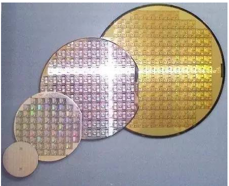
The verification of the physical layout is the completion of the whole chip design phase, and the following is the chip manufacturing. The physical layout is given as a GDS II file to a Foundry, or Foundry, which makes actual circuits on a silicon wafer, packages them and tests them, and you get the actual chip you see.
Process documentation for chip design
In the important design links of chip design, such as synthesis and timing analysis, layout drawing, etc., process library files are needed. However, people often lack understanding of process documents, so it is difficult to learn something about chip design by themselves. For example, learning layout design is just a paper project without a process chart library file. This article mainly introduces the process library related knowledge.
The process documentation is provided by the chip manufacturers, so it is necessary to have a general understanding of the domestic and international chip manufacturers. Internationally, there are major semiconductor manufacturers such as TSMC, Intel and Samsung. In China, there are mainly SMIC, China Resources Shanghai, Shenzhen Founder and other companies. These companies provide relevant process library documents, but the premise is to cooperate with these companies to obtain, these process documents are confidential documents.
The complete process library file is mainly composed of:
1, simulation process library, mainly support the two software spectre and hSPICE, suffix SCS -- Spectre, lib -- hSPICE use.
2, the analog version of the map library file, mainly for cadence map drawing software, the suffix tf, DRF.
3. Digital comprehensive library, mainly including timing series library, basic netlist components and other related comprehensive and chronological analysis required library files. It is mainly used for DC software synthesis and PT software timing analysis.
4. Digital map library, mainly for cadence Encounter software for automatic layout and routing, of course, automatic layout and routing tools will also use timing library, integrated constraint files, and so on.
5, map verification library, mainly DRC,LVS check. Some specialized support Calibre, and some specialized support Dracula, Diva and other map inspection tools. Each library file has a corresponding PDF description document.
The reverse design will use process library files 1,2,5, 3 and 4 will not be used. A forward design (a forward design that starts with code) requires all the files. Due process documentation occupies very important position in the chip design, key design at every link are used, plus its confidential property, so it is difficult to find the complete process documents on the network for individual learning, have a cadence EETOP open for personal learning process library files can be convenient for everybody to learn, but also seems to be incomplete.
Synthesis of chip design
What is synthesis? Synthesis is the process of transforming/mapping RTL-level Verilog code into circuits represented by basic gate level units using the Design Compiler tool. The basic gate units are the nand gates, or nand gates, registers, etc., but these gate units have been made into a standard library of units that we can call directly with software, rather than having to call the gate units ourselves to build the circuit. In simple terms, the Design Compiler software does the job of translating code into actual circuits, but it's not just about translating, it's about optimizing the circuits and timing constraints to make them fit the performance requirements we've set. As mentioned earlier, the software is constraint driven, so where does the constraint come from? The answer is, design specifications. Every chip design project will have a project specification, which is developed at the beginning of the chip design, in the overall planning (see above) steps. Specific constraints need to be carefully considered during the integration process. General process of synthesis:
1. Pre-synthesis process;
2. Impose design constraint process;
3. Design synthesis process;
4. Post-synthesis process.
PS, a prerequisite for using Design Compiler software is to learn to use DC TCL scripts.
Pre-synthesis process. This part mainly consists of preparing the library files (including process library, link library, symbol library, and comprehensive library) used by the comprehensive process, design input files, and setting environmental parameters.
Impose design constraints on the process. This part is mainly about writing constraint files using DC TCL scripts. Specific constraint items can be divided into three categories:
A, area constraint, define clock, constrain input/output path;
B. (environment attribute), constrains input driver, constrains output load, sets working conditions (best, typical, worst case), and sets line load model;
C. (advanced clock constraint), the clock jitter, offset, clock source delay, synchronous multi-clock, asynchronous clock, multi-cycle path, these categories of detailed constraints.
So much for the constraints. A detailed TCL script constraint file contains almost all of the above constraints. There is a constraint behind the model.
Design the integrated process. It mainly introduces the circuit module Design planning (for better constraint), the process of Design Compiler comprehensive optimization (three optimization stages, structure level, logic level, gate level), the specific process of time sequence analysis and other detailed information in the comprehensive process.
Post synthesis process. How do you look at the results of the synthesis? How do you resolve the timing violations? That's what the post-synthesis process is all about. After the synthesis, through the analysis of the synthesis report, we can know how the circuit synthesis result, according to the requirements that do not meet, re constraint, or even redesign the circuit. In particular at this stage is a comprehensive forecast, because when writing comprehensive constraint of the script, you need to determine the constraint, the specification is generally not able to involve so details section, so need a comprehensive forecast according to the actual circuit, after this step is in the code, and test at the same time, to roughly estimate the circuit is in line with the requirements, In this case, the pre-synthesis process is the same as the formal synthesis, but the requirements are much more relaxed. The timing violation requirement is about 10%-15%, that is to say, it does not matter if 10%-15% of the circuit does not meet the timing.
conclusion(iPCB.com)
The process of chip design is very complex, this article is also a simple chip design process comb again, the complex will not repeat.