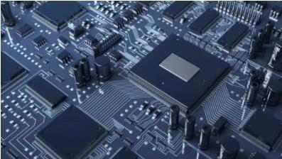
IC chip packaging and testing process:
Process

IC Package refers to the chip (Die) and different types of frame (L/F) and plastic sealing material (EMC) formed by different shapes of the Package body.
There are many kinds of IC Package, which can be classified as follows:
According to packaging materials, it can be divided into:
Metal packaging, ceramic packaging, plastic packaging


Metal packaging is mainly used in military or aerospace technology, no commercial products;
Ceramic packaging is better than metal packaging, also used in military products, a small amount of commercial market;
Plastic packaging for consumer electronics, its low cost, simple process, high reliability and occupy the vast majority of the market share;
According to the connection mode with PCB board, it can be divided into:
PTH packaging and SMT packaging


PTH-Pin Through Hole;
SMT-Surface Mount Technology.At present, most IC on the market are adopted for SMT type.
According to the package appearance, it can be divided into:
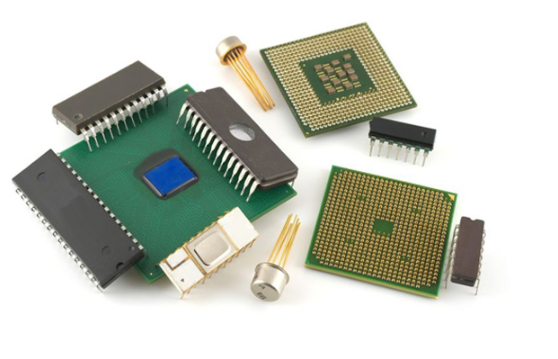
SOT, SOIC, TSSOP, QFN, QFP, BGA, CSP, etc.
Two key factors determine the form of encapsulation:
Encapsulation efficiency. Chip area/package area, as close as possible to 1:1;
Pin number. The more pins, the more advanced, but the difficulty of the process also increases accordingly;
Among them, CSP, due to the use of Flip Chip technology and bare Chip package, Chip area/package area =1:1, which is the most advanced technology at present.
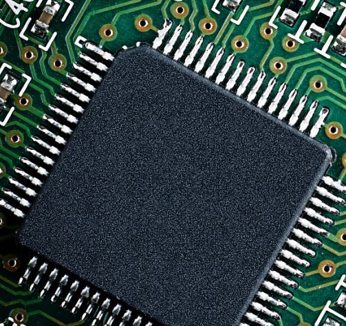
QFN -- Quad Flat no-lead Package QFN -- Quad Flat No-lead Package
SOIC - Small Outline IC Package
TSSOP - Thin Small Shrink Outline Package
QFP - Quad Flat Package
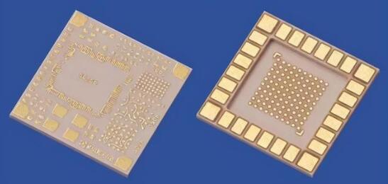
BGA -- Ball Grid Array Package
CSP - Chip Scale Package Chip Scale Package
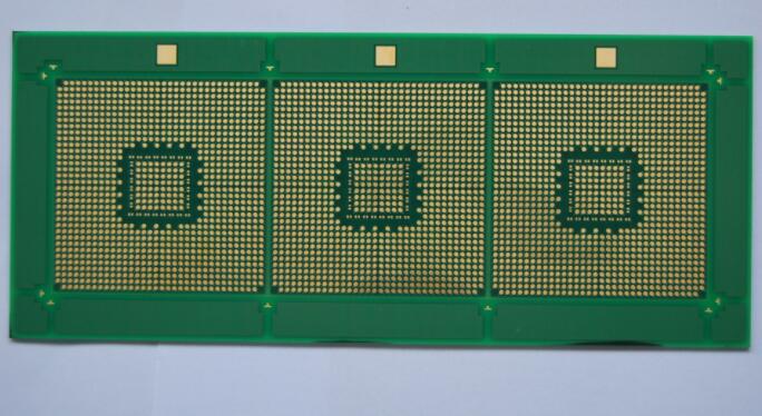
IC Package Structure

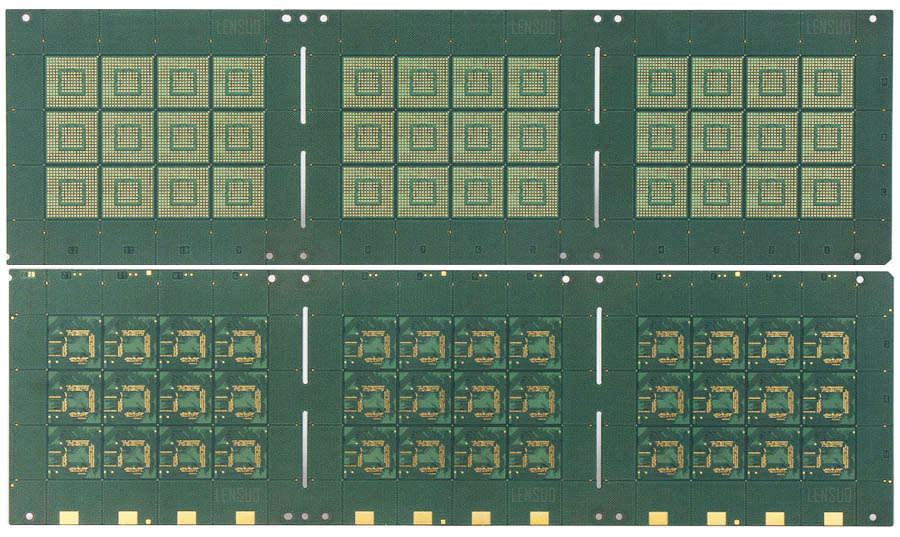
Raw Material in Assembly【Wafer】


【Lead Frame】

Provides circuit connection and Die fixation;
The main material is copper, which will be coated with silver and NiPdAu.
The L/F process includes Etch and Stamp;
Easy to oxidize, stored in a nitrogen cabinet, the humidity is less than 40%RH;
Except BGA and CSP, other packages will use Lead Frame, while BGA will use Substrate;
【Gold Wire】

To realize the electrical and physical connection between the chip and the external lead frame;
Gold thread is 99.99% high purity gold;
At the same time, due to cost considerations, copper wire and aluminum wire processes are currently used. The advantage is that the cost is reduced, and the process difficulty is increased, the yield is reduced;
The wire diameter determines the conductable current; 0.8mil, 1.0mil, 1.3mils, 1.5mils and 2.0mils;
The main components of the Mold Compound/epoxy resin are: epoxy resin and various additives (curing agent, modifier, Mold stripping agent, dyeing agent, flame retardant agent, etc.);
The main functions are as follows: The Die and the Lead Frame are wrapped in the molten state to provide physical and electrical protection and prevent external interference;
Storage conditions: 5° below zero, 24 hours under normal temperature;
【Epoxy】

Epoxy resin filled metal powder (Ag); It has three functions: fixing the Die on the Die Pad; Heat dissipation, conductive effect;
-50° below storage, before use back temperature 24 hours;


FOL-Front of Line

FOL-Back Grinding
The Wafer from the Wafer factory is ground on the back to reduce the Wafer thickness required for packaging (8mils~10mils).
When grinding, it is necessary to put tape on the Active Area to protect the circuit and grind the back at the same time. After grinding, remove the tape and measure the thickness;

FOL– Wafer Saw
The wafer is pasted on a blue film (Mylar) so that it will not fall apart even after being cut open;
Cut the whole Wafer into independent Dice through Saw Blade to facilitate Die Attach and other processes behind.
Mainly clean the dust produced by Saw, clean the Wafer;


FOL -- 2nd Optical Inspection
The main purpose is to inspect the appearance of Wafer under microscope after Wafer Saw to see if there is any waste.

FOL– Die Attach
Chip picking process:
1. Ejector Pin jacking up the chip from Mylar under the wafer, making it easy to break away from the blue film;
2.The chip is picked up from above to complete the transportation process from Wafer to L/F;
3. Collect the chip Bond on the L/F Pad with silver paste with a certain force, and the specific position is controllable;
4, Bond Head Resolution: x-0.2um; Y - 0.5 um; Z - 1.25 um;
5. Bond Head Speed: 1.3m/s;

FOL– Epoxy Cure

175°C, 1 hour; N2 environment, to prevent oxidation:
Die Attach quality check:
Die Shear


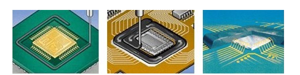
FOL– Wire Bonding
High purity gold (Au), copper (Cu) or aluminum (Al) wires are used to connect the Pad and the Lead by welding. The Pad is the external connection point of the circuit on the chip, and the Lead is the connection point on the Lead Frame.
W/B is the most critical process in the packaging process.

FOL– 3rd Optical Inspection

EOL– End of Line

EOL– Molding


EOL– Laser Mark

Laser lettering on the front or back of Package. The content includes: product name, production date, production batch, etc.

EOL– Post Mold Cure
Used for curing plastics after Molding to protect IC internal structure and eliminate internal stress. Cure Temp: 175 + / - 5 ° C; Cure Time: 8 HRS

EOL– De-flash
Purpose: the purpose of de-Flash is to remove excess Molding between the leads around the tube body after Molding; Methods: Soak with weak acid and rinse with high pressure water.

EOL– Plating
Using metallic and chemical methods, a coating is applied to the surface of the Leadframe to prevent the effects of the external environment (moisture and heat). And make the components on the PCB board easy to weld and improve electrical conductivity.
There are generally two types of electroplating:
Pb-free: lead-free electroplating, using is >99.95% of high purity Tin (Tin), for the current widely used technology, in line with the RoHS requirements;
It's a tin-lead alloy. Tin accounts for 85%, and Lead accounts for 15%. Because it does not conform to RoHS, it is basically eliminated at present.


EOL– Post Annealing Bake
Objective: Let the product after lead-free electroplating bake at high temperature for a period of time, in order to eliminate the potential Whisker Growth problem of electroplating; Condition: 150 + / - 5 - c; 2Hrs;

The process of cutting the Lead Frame of a slice into individual units (IC); Form: Shape the IC product after Trim, reach the shape required by the process, and put it into the Tube or Tray;

EOL– Final Visual Inspection
Inspect the product appearance under a low power magnifying glass.
5. Focus on potential waste products from EOL process such as Molding defects, plating defects, Trim/Form defects etc.