Semiconductor chips - How should we break the Situation
Chip, also known as Integrated Circuit Board - IC, is a form of semiconductor components, non-active components and other small scale, can be a large number of micro junction transistors integrated into a small chip.

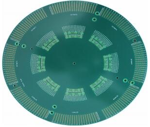
Integrated Circuit Board - IC
So chip is composed of one junction transistor, all kinds of solid state semiconductor components (diode, junction transistor), mid and late 2000 semiconductor technology progress to improve for Integrated Circuit chip's become possible, from manual assembly using the clutch of electronic components Integrated Circuit Board is more reliable, high performance (small size short way to quickly switch low power components, Low energy consumption), low cost (photo board technology, high production rate).
In the past, nations and communities of people fought for food resources such as land, population, burning materials, markets and so on. These resources required basic transportation links, so we built many roads and Bridges to carry these resources and make them useful. Since the second World War, basic science has not been fundamentally broken, and many fields, such as energy, matter and materials, have remained stagnant. It is seeking a better survival, and digital infrastructure has become the new high point. ation
1, Digital infrastructure:
In the era of digital economy, we have become the central production factor and strategic resource. The basic software and hardware such as network, storage, computing and application around the whole life cycle of digital has become new infrastructure that is indispensable for production, survival and social form progress. Through these new infrastructure, we have successfully realized the management of the "invisible world" behind the physical space. Based on the current international momentum and the impact of the epidemic, digital infrastructure can work, stimulate investment, steadily participate in work and revitalize the economy. Unlike the traditional infrastructure in the past, digital infrastructure is the most dynamic economic field at present.
Digital infrastructure is the cornerstone and guarantee of the progress of digital economy and a new driving force of high-quality economic progress. Therefore, in the foreseeable future, the world will usher in a trend of vigorously investing in digital infrastructure.
2, Communication and Computing:
The application of digital infrastructure revolves around communication and computing power, which translates into 5G and chip as we clearly know. 5G communication reputation links and summarizes the values gathered together, and computing power is the disposal of the summarized information.
In the traditional economy, production lines, machines and various vehicles are used as production tools, while land, productivity and fossil combustion materials become the central production factors; Corresponding to the new digital infrastructure, AI, 5G, Internet of things and cloud computing have become new production tools, while computing power and value have become the central production factors of the above-mentioned tools. Computing power and value have become the commanding heights of current world competition.
-. Communication:
In the field of communication, China is very worthy of it. Up to now, Huawei has the largest number of 5G patents in the world, and its comprehensive technology is at the level of the world. However, we can't help being optimistic in the field of chips, especially high-end chip s. Although we have a large number of semiconductor chip companies, such as SMIC international and China microelectronics, they are not specialized in all fields, The chip industry needs the coordinated progress of the whole industry chain, especially in one key technology.
-. Calculation:
In the current era of the Internet of things, it is extremely convenient to obtain trust information. Even in the foreseeable future, when the information is vast enough, the computing power is strong enough, and the country's decisions can be delivered to the computer, all we have to do is formulate operation rules, that is, algorithms. Multi industry information enables collaborative computing to sprout new needs, production capacity and market, and help the world's economic progress. At that time, the game between countries will be very large, and it is likely to become between two supercomputers. Who can obtain more data, support scientific algorithms, and finally stand out and make accurate choices through stronger computing power.
IDC, an international numerical enterprise, predicts in advance that by 2023, the output value of digital economy will account for 67% of China's GDP. Strong and independent computing power will become the cornerstone of China's economic progress, and the investment and development of computing power of the central factor will become China's long-term plan. There is no doubt that the countries occupying these two fields will achieve important and practical power in the next few decades, Even the world order after the voting day.
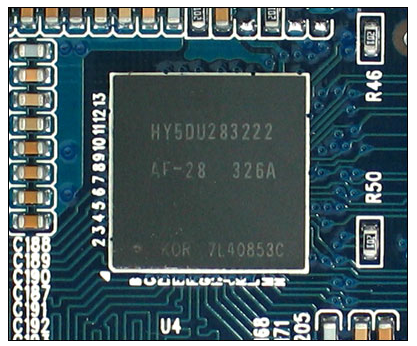
Semiconductor is a kind of thing whose conductivity is between conductor and insulator (which will be discussed in detail below). It was not widely licensed until the high purification technology of materials was improved in the 1930s. Semiconductors are mainly composed of integrated circuits, photoelectric components, discrete components and sensors. Because the integrated circuits account for more than 80% of the components, semiconductors are commonly referred to as integrated circuits. The integrated circuit is divided into micro processor, memory, thinking law unit and imitation component. So we also turn it into a chip.
Development history of chip
Intel is a chip giant in the PC field. Its development history basically represents the development history of chips. Let's take a look at its development history:

History of Chip
1. In 1971, Intel's first commercial processor 4004 came out, integrating 2250 crystal tubes and 60000 operations per second. Its exposure was revolutionary, brought the subsequent computer and Internet revolution, and continued to change the whole world.
2. In 1978, Intel's famous 8086 processor came out and was applied to IBM computer in 1981. Then there are subsequent models such as 80286.
3. In 1985, Intel researched and manufactured the first 32-bit processor 80386. Relying on the compatibility and cooperation with IBM PC, Intel firmly established the leading position in the compatible machine market and entered the Chinese market in the same year. There are also improved models 80486, 586, etc. Xiaosheng remembered that the first Win95 processor computer used in an hour is the 80486 series chip.
4. In 1993, Intel launched Pentium. At this time, the number of crystal tubes reached 3.2 million. The experience of floating-point operation was greatly strengthened, and the functions of image, sound, film and television were fully and successfully realized. In the following ten years, the updated numbers continued one after another, and Intel has become the representative name of high-end chips.
5. In 2001, Intel's first 64 bit processor Itanium was born, which is mainly used for high-end company level computing background, that is, servers, surpassing peers and becoming the leader of server chips.
6. In 2006, the core dual core processor that we know well came out, that is, our so-called I3, i5 and i7 series. Of course, the Core i7 was launched in 2008 and is the first quad core processor. The core series is durable. Up to now, our private computers basically use the core series (other variants of AMD or Intel on the core).
7. In 2014, Intel launched Xeon E7 series processors, with up to 15 processor centers becoming the largest number of processors in Intel center. Xeon is mainly used in the server field and can be applied to Internet processing engineering, image and multi TV stations, etc.
8. In 2017, after Intel bought Mobileye from various places, it began to make progress in the direction of "algorithm + chip" integrated AI. In the environment of intelligent AI, NVIDIA and Intel are using technologies such as deep learning neural organ network to make AI chips and seize the new market.
Throughout the development history of integrated circuits in the past 30 years, the number of crystal tubes has doubled every 1.5 years. With the increase of the size of unit plane or object surface, the overall size of the chip has changed from large to small, and the surface of monomer cost and switching power has decreased. At the same time, all performance indexes have been strengthened, that is, the number and performance of crystal tubes of the chip have doubled every 24 months, Adhering to MOLLE's law, the history of chip progress is the history of Integrated Circuits.
It can be said that the hardware of the IT industry is based on the semiconductor industry, and the semiconductor is composed of crystal tubes (including diodes, tubes with three electrodes, field effect tubes, thyristors, etc., sometimes especially bipolar components). Let's start with semiconductors and crystal tubes (other principles are almost the same).
1. Semiconductor:
When it comes to chips, we have to mention semiconductors. In fact, the discovery of semiconductors has also been developed by quantum mechanics. Let's mention it from the level of physical atoms. We all know that other elements except h and he are in the stable state of outer layer 8 electrons. Chemical knowledge also tells us that the electrostatic force (chemical bond) that enables the two elements to be connected has ionic bond and covalent bond (metal bond is roughly similar to covalent bond).
Ionic bonds generally exist between metals and nonmetals. For example, Na atom misses an electron and becomes Na + particle, Cl atom obtains an electron and becomes CL particle, and the two atoms become heterosexual charges. Through current, they are attracted together by magnetic energy and become NaCl, that is, salt and sodium chloride; Covalent bonds generally require the bonding of non-metallic elements. Different atoms can form electron pairs side by side with extra nuclear electrons, so that the outermost layer forms an 8-electron stable state, such as nitrogen.
At present, we have carefully checked that there are only four electrons in the outermost layer of group C elements in the periodic table, which is not easy to miss or obtain electrons. This is the concept of semiconductor. However, with the increase of the number of electron layers, it will become more and more easy to miss electrons in this group of elements (Si later elements Ge, Sn, Pb, etc.), It is found that silicon Si has become the best semiconductor material in our eyes because of its appropriate number of electron layers and the number of electrons in the outermost layer. This is also the origin of the "Silicon Valley" where the world's high-tech industries gather. The "Silicon Valley" is also the first place to study and produce silicon-based semiconductor chips, because it is named.
2. Crystal tubes and Integrated Circuits:

Crystal Tubes & IC
Diode is one of the crystalline tubes. It is an electronic component that can conduct electricity in one direction made of semiconductor materials (silicon, selenium, germanium, etc.). That is, it turns on when the anode and cathode of the diode are given a forward voltage and ends when the reverse voltage is given, which is equivalent to the connection and breaking of a switch. Now we have the most basic signal difference. For example, we record the current conduction as 1 and the fracture as 0. This is the computer language 0 and 1 that we know very well. Now C language, C + +, JS and H5 have become languages, which is also a way to translate such 01 languages into a way that we can understand and edit conveniently.
After the birth of the diode, we can preset the original thinking law. Everyone who has studied the course of semi-automatic control principle knows that there is an and or non gate circuit (for example, the and gate successfully realizes the output of 1 at the same time). All kinds of gate circuits are gathered in parallel and series. The seemingly simple thinking law gate circuits can successfully realize very complex calculation after hundreds of millions of arrangement and combination of gate circuits are gathered together (where the arrangement and combination preset of gate circuits is not only the preset of chip technology, but also the central element of voting chip performance, It needs the accumulation of technology for a long time), and the chip is the aggregation of this kind of computing circuit, that is, integrated circuit IC.
The manufacturing process of chip is relatively complex, but it is generally divided into three steps:? Design, production and packaging test.
1, Preset:
Front end preset, front simulation, back-end preset, verification, post simulation, signoff search, and then send the set statistics to the agent factory.
We need to know a principle about presetting. To successfully realize a certain function, chip presetting must rely on a preset architecture. So far, the mainstream chip architectures include x86 (exclusive to Intel and AMD, dominating the PC market), arm (mobile convenience facilities), risc-v (rising star, widely used in intelligent Wearable facilities), MIPs (mainly used in gateways Set top box), because the arm architecture has a unique place of low power consumption and low cost, it is especially popular with mobile devices such as mobile phones (arm and x86 architecture are the two largest architectures with the largest market share).
The chip architecture mentioned above is only a prerequisite. EDA software is required for the whole preset process of the chip. In short, EDA software can be understood as our commonly used CAD software, because a chip circuit is very complex and small, which contains tens of billions of components. Incorrect placement of a component or circuit may make the whole chip unable to run. EDA software can semi automatically preset the process to ensure the operation of the chip. The chip preset party only needs to vote on the preset of several key positions.
2, Production:

Production Line
Oxygenation - film deposition - lithography - etching - ion perfusion - cleaning.
First, we extract high purity simple silicon from silicon dioxide, that is, sand at high temperature. The simple silicon is a crystalline structure with neat atoms and covalent bonds to form large molecules. Office workers cut silicon into round slices to produce chips.
Apply gelatin evenly on the silicon wafer, control the light (lithography machine) mapping, change the properties of gelatin at the specially designated position (soluble in water), and then rinse with water to obtain the groove of silicon.
When impurities such as photosensitive polysilicon layer are added to the specially designated area, such as scanning and phosphorus in the diode, the thinking law circuit is continuously formed in the groove, commonly known as particle perfusion.
The rest of the places can also be covered by photosensitive coating, and the silicon can be corroded with corrosive solution to form crystal tubes.
Of course, you can also mix metal materials to form wires, electricity or resistance.
This process can be repeated many times (generally no less than 20) to obtain the integrated circuit we expect, a large crystal disk containing many chips.
3, Package test:
As mentioned above, after the chip is produced, it is not a finished product, but a large wafer, which needs to be tested, cut and encapsulated by the chip tester.
Satisfactory testing can make products that do not meet quality standards obsolete before they reach users, which is crucial to increasing production and quality and establishing a virtuous circle of production and marketing. The testing machine is a successful test to verify whether the chip meets the preset purpose, study the impact of background changes on it, and the uneven life span.
By 2019, China had spent more than $300 billion on imported chips (only more than $200 billion on fuel), and purchased a total of one-third of the world's chips, of which more than 90% depended on imports. It can be seen that our dependence on chips is still quite large. To study the current situation of semiconductor chips in China, we must first look at the division of labor in the whole process of the chip industry.
World chip industry chain:
China's Precision company, overseas fruit, AMD, Qualcomm and other famous manufacturers often only make preset, which we call fabless chip preset; After preset, deliver the drawings to a third-party chip manufacturing foundry such as TSMC or Samsung; After production, it is not a finished product, but a large round silicon junction crystal. It has to be delivered to day color and security. Such enterprises use EDA software to test, cut and package, and finally form the chips we usually see.
Most chip production processes are described above, but there are rare exceptions. For example, the whole process of super large enterprises such as Intel and Samsung is balanced by themselves, that is, the preset, production, test and packaging are all done by themselves. We generally call this standard style IDM standard style. In fact, at first, we all produced chips in IDM standard style, but later, we thought about the cost and speed. After all, setting up a production line by ourselves is too expensive, and the upgrading is fast. After the facilities are put there for depreciation.
Then, the need led to the emergence of an enterprise such as TSMC, which greatly increased its production capacity on the premise of cost control. However, this has also brought another change, that is, the threshold group of the chip industry has been reduced. Once there were not hundreds of billions of people who could not touch the threshold of the chip industry. Now it only needs to invest more than a dozen to billions of chip preset development to find someone to make chips.
Comparison between China's chip preset, production and test packaging and the world standard:
After finishing the world chip industry chain, let's go back to the process flow of the chip itself, that is, preset, production and packaging testing. Let's analyze it from these three dimensions.
1, Chip preset:
Chip preset is generally divided into: front-end preset, front-end simulation, back-end preset, verification, post simulation, signoff investigation, and then send the set statistics to the OEM.
As mentioned above, many large companies including Huawei Hisilicon only do chip preset, so Hisilicon is basically a chip preset enterprise.
1. Arm architecture:
As mentioned above, up to now, the mainstream chip architectures include x86 (exclusive to Intel and AMD, dominating the PC market), arm (mobile convenience facility), risc-v (rising star, widely used in intelligent wearable facilities), MIPs (mainly used in gateways and set-top boxes), because arm architecture has low power consumption The unique place of low cost is particularly affected by the blue eye of mobile facilities such as mobile phones (arm and x86 architecture are the two largest architectures in terms of market share).
Our Precision company came from the secondary research and development based on the public version architecture of arm enterprise. Although arm is a British enterprise and claims not to be affected by the commercial affairs department of country a, arm's behavior has been unstable in the past year. So far, it has been reported that it will be bought by NVIDIA from all over the world, which also seems very unreliable. If we do not allow Precision companyto independently preset the chip of the next generation instruction set, the degree of difficulty is very high.
2. EDA preset:
The chip structure is the presupposition premise. When you choose a building site and foam cement, you also need a specific architectural plan, that is, chip presetting. In this process, we have talked about the whole journey of requiring EDA software (roughly similar to CAD software in the construction industry). As mentioned above, EDA software can semi automatically preset the chip of the whole process to ensure its successful operation. The designers only need to change several key positions, which greatly reduces the uncontrollable risk.
Our Precision company mainly uses the software of Mingdao international, Xinsi science and technology and Kaideng electronics. It happens that these three are the largest EDA software enterprises in the world, and all of them are American enterprises.
Smart EDA software providers also provide free EDA software to foundry factories such as TSMC, requiring the foundry to provide EDA software with numerical packages of basic information of components and thinking law units such as crystal tubes, MOS tubes, resistors, capacitors, etc. the numerical packages are continuously optimized and updated many times (sometimes a month) and form verification and binding with the software, Therefore, it basically only supports the latest version. Unlike pirated software, we can still use the old version without updating it after the prohibition law. If we don't need the latest version of software to verify the chip, it is likely that the preset chip can't run, resulting in streaming failure, and a streaming failure means that hundreds of millions of funds have been lost, and the cost risk is very high.
Huada Jiutian is finally the leading company of EDA software in China. Through years of progress, it has been able to take charge of some fields. However, as mentioned above, like semiconductor chip s, it needs the cooperation of the whole process to cover the preset process of the whole high-end chip, and we can only cover some points.
2, Chip fabrication:
The process of chip fabrication can be roughly divided into: oxygenation - film deposition - lithography - etching - ion perfusion - cleaning;
In the field of chip manufacturing, TSMC is undoubtedly the strongest company in the world. Its strong technology and leading capacity ensure its leading position. However, all this is based on the use of a large number of American semiconductor facilities. It can be said that there will be no TSMC today without the support of American technology. Therefore, if a ban is issued in country a, TSMC will be able to choose not to process chips for us after weighing the order and its foundation technology.
You might say that we still have SMIC? After years of hard work, SMIC international, which was listed in 2004, finally conquered the node of 14nm process in 19 years, which was finally a major breakthrough. However, first of all, we have to realize that TSMC has supplied 7 nm chips to fruits in 18 years, which lags behind by at least two generations in terms of process technology. Secondly, even if we can accept products that are not so good in size, performance and continuous navigation, SMIC can not do it for us. In the above-mentioned chip manufacturing process, in the etching link, our microelectronics has been able to apply more advanced technology to 7Nm and 5nm production lines. However, in addition, it lags behind the world average level. In the production link, there are a large number of technologies from the United States. For example, SMIC has applied the scheme of American applied materials enterprises. Therefore, if country a really has a ban, SMIC can not make chips for Huawei.
Lithography:
Secondly, only one key technology - lithography can be mentioned in chip fabrication. A lithography machine projects a circuit diagram onto a silicon wafer covered with photoresist; The etching machine corrodes the parallel branch circuit diagram on the silicon wafer that has just drawn the circuit diagram. The two facilities complement each other, and one cannot be missing.
EUV lithography technology has a high degree of difficulty (the improved version of DUV has successfully changed from large to small wavelength after suppressing liquid metal tin, which will not be described in detail here). The development began more than 20 years ago, with the participation of nearly 40 countries, including all European countries. However, only the United States firmly maintained that in the end, the degree of technical difficulty is more than making atomic bombs. In the current chip, we have to perform at least 20 times of lithography (one layer at a time), and when we enlarge the drawing of a single etching layer many times, it is more complex than the topographic map of the whole new york city and suburbs. Imagine recording the whole new York and suburban topographic map on a chip with a plane or object surface size of only 100 square mm (the size of a crystal tube is less than one of the extremes of a hair diameter). How complex the structure is can be imagined.
Therefore, photolithography is a very complex and key technology. Its precision and sharpness directly vote on the computing experience and quality of the chip. Only the more accurate etching ability can successfully realize the idea of the circuit designer at the micro scale. There is no doubt that lithography technology is the forefront of competition among countries in the chip lithography period.
The cutting-edge field of lithography technology is monopolized by the Dutch enterprise ASML (ASML), and its 5nm lithography machine has been put into use. This year, TSMC's A14 processor, Qualcomm Xiaolong 875 series and mascot 9000 processor were all produced by this facility. Up to now, China's lithography machine is the 28nm process of microelectronics. There is an era of experience difference in development and two times of experience difference in mass production. As for many other links, they have even just begun to go.
3, Package test:
As mentioned above, after the chip is produced, it is not a finished product, but a large wafer, which needs to be tested, cut and encapsulated by the chip tester.
Satisfactory testing can make products that do not meet quality standards obsolete before they reach users, which is crucial to increasing production and quality and establishing a virtuous circle of production and marketing. The testing machine is a successful test to verify whether the chip meets the preset purpose, study the impact of background changes on it, and the uneven life span.
By 2019, China had spent more than $300 billion on imported chips (only more than $200 billion on fuel), and purchased a total of one-third of the world's chips, of which more than 90% depended on imports. It can be seen that our dependence on chips is still quite large. To study the current situation of semiconductor chips in China, we must first look at the division of labor in the whole process of the chip industry.
World chip industry chain:
China's Precision company, overseas fruit, AMD, Qualcomm and other famous manufacturers often only make preset, which we call fabless chip preset; After preset, deliver the drawings to a third-party chip manufacturing foundry such as TSMC or Samsung; After production, it is not a finished product, but a large round silicon junction crystal. It has to be delivered to day color and security. Such enterprises use EDA software to test, cut and package, and finally form the chips we usually see.
Most chip production processes are described above, but there are rare exceptions. For example, the whole process of super large enterprises such as Intel and Samsung is balanced by themselves, that is, the preset, production, test and packaging are all done by themselves. We generally call this standard style IDM standard style. In fact, at first, we all produced chips in IDM standard style, but later, we thought about the cost and speed. After all, setting up a production line by ourselves is too expensive, and the upgrading is fast. After the facilities are put there for depreciation.
Then, the need led to the emergence of an enterprise such as TSMC, which greatly increased its production capacity on the premise of cost control. However, this has also brought another change, that is, the threshold group of the chip industry has been reduced. Once there were not hundreds of billions of people who could not touch the threshold of the chip industry. Now it only needs to invest more than a dozen to billions of chip preset development to find someone to make chips.
Comparison between China's chip preset, production and test packaging and the world standard:
After finishing the world chip industry chain, let's go back to the process flow of the chip itself, that is, preset, production and packaging testing. Let's analyze it from these three dimensions.
1, Chip preset:
Chip preset is generally divided into: front-end preset, front-end simulation, back-end preset, verification, post simulation, signoff investigation, and then send the set statistics to the OEM.
As mentioned above, many large companies including H-Hisilicon only do chip preset, so Hisilicon is basically a chip preset enterprise.
1. Arm architecture:
As mentioned above, up to now, the mainstream chip architectures include x86 (exclusive to Intel and AMD, dominating the PC market), arm (mobile convenience facility), risc-v (rising star, widely used in intelligent wearable facilities), MIPs (mainly used in gateways and set-top boxes), because arm architecture has low power consumption The unique place of low cost is particularly affected by the blue eye of mobile facilities such as mobile phones (arm and x86 architecture are the two largest architectures in terms of market share).
Our High Precision company came from the secondary research and development based on the public version architecture of arm enterprise. Although arm is a British enterprise and claims not to be affected by the commercial affairs department of country a, arm's behavior has been unstable in the past year. So far, it has been reported that it will be bought by NVIDIA from all over the world, which also seems very unreliable. If we do not allow Huawei to independently preset the chip of the next generation instruction set, the degree of difficulty is very high.
2. EDA preset:
The chip structure is the presupposition premise. When you choose a building site and foam cement, you also need a specific architectural plan, that is, chip presetting. In this process, we have talked about the whole journey of requiring EDA software (roughly similar to CAD software in the construction industry). As mentioned above, EDA software can semi automatically preset the chip of the whole process to ensure its successful operation. The designers only need to change several key positions, which greatly reduces the uncontrollable risk.
Our High Precision company mainly uses the software of Mingdao international, Xinsi science and technology and Kaideng electronics. It happens that these three are the largest EDA software enterprises in the world, and all of them are American enterprises.
Smart EDA software providers also provide free EDA software to foundry factories such as TSMC, requiring the foundry to provide EDA software with numerical packages of basic information of components and thinking law units such as crystal tubes, MOS tubes, resistors, capacitors, etc. the numerical packages are continuously optimized and updated many times (sometimes a month) and form verification and binding with the software, Therefore, it basically only supports the latest version. Unlike pirated software, we can still use the old version without updating it after the prohibition law. If we don't need the latest version of software to verify the chip, it is likely that the preset chip can't run, resulting in streaming failure, and a streaming failure means that hundreds of millions of funds have been lost, and the cost risk is very high.
HD JT is finally the leading company of EDA software in China. Through years of progress, it has been able to take charge of some fields. However, as mentioned above, like semiconductor chips, it needs the cooperation of the whole process to cover the preset process of the whole high-end chip, and we can only cover some points.
2, Chip fabrication:
The process of chip fabrication can be roughly divided into: oxygenation - film deposition - lithography - etching - ion perfusion - cleaning;
In the field of chip manufacturing, TSMC is undoubtedly the strongest company in the world. Its strong technology and leading capacity ensure its leading position. However, all this is based on the use of a large number of American semiconductor facilities. It can be said that there will be no TSMC today without the support of American technology. Therefore, if a ban is issued in country a, TSMC will be able to choose not to process chips for us after weighing the order and its foundation technology.
You might say that we still have SMIC? After years of hard work, SMIC international, which was listed in 2004, finally conquered the node of 14nm process in 19 years, which was finally a major breakthrough. However, first of all, we have to realize that TSMC has supplied 7 nm chips to fruits in 18 years, which lags behind by at least two generations in terms of process technology. Secondly, even if we can accept products that are not so good in size, performance and continuous navigation, SMIC can not do it for us. In the above-mentioned chip manufacturing process, in the etching link, our microelectronics has been able to apply more advanced technology to 7Nm and 5nm production lines. However, in addition, it lags behind the world average level. In the production link, there are a large number of technologies from the United States. For example, SMIC has applied the scheme of American applied materials enterprises. Therefore, if country a really has a ban, SMIC can not make chips for Huawei.
Lithography:
Secondly, only one key technology - lithography can be mentioned in chip fabrication. A lithography machine projects a circuit diagram onto a silicon wafer covered with photoresist; The etching machine corrodes the parallel branch circuit diagram on the silicon wafer that has just drawn the circuit diagram. The two facilities complement each other, and one cannot be missing.
EUV lithography technology has a high degree of difficulty (the improved version of DUV has successfully changed from large to small wavelength after suppressing liquid metal tin, which will not be described in detail here). The development began more than 20 years ago, with the participation of nearly 40 countries, including all European countries. However, only the United States firmly maintained that in the end, the degree of technical difficulty is more than making atomic bombs. In the current chip, we have to perform at least 20 times of lithography (one layer at a time), and when we enlarge the drawing of a single etching layer many times, it is more complex than the topographic map of the whole new york city and suburbs. Imagine recording the whole new York and suburban topographic map on a chip with a plane or object surface size of only 100 square mm (the size of a crystal tube is less than one of the extremes of a hair diameter). How complex the structure is can be imagined.
Therefore, photolithography is a very complex and key technology. Its precision and sharpness directly vote on the computing experience and quality of the chip. Only the more accurate etching ability can successfully realize the idea of the circuit designer at the micro scale. There is no doubt that lithography technology is the forefront of competition among countries in the chip lithography period.
The cutting-edge field of lithography technology is monopolized by the Dutch enterprise ASML (ASML), and its 5nm lithography machine has been put into use. This year, TSMC's A14 processor, Qualcomm Xiaolong 875 series and mascot 9000 processor were all produced by this facility. Up to now, China's lithography machine is the 28nm process of microelectronics. There is an era of experience difference in development and two times of experience difference in mass production. As for many other links, they have even just begun to go.
3, Package test:
Friends who understand the chip may think that China is in the first column in the world in the packaging and testing link. However, the real situation of the matter is that the polishing testing machine is monopolized by Japanese and American companies, where tereda and Kexiu semiconductor from the United States occupy more than half of the domestic sealing and testing facilities, and the localization rate of semiconductor testing facilities is not sufficient by 10%.

Packaging Test
After the gap between China's semiconductor chips and the world standards in terms of preset, production and packaging testing, we should not be too optimistic. In fact, we are not without experience in EDA, production, lithography and OEM. Huada Jiutian, Zhongwei electronics, Hisilicon and other companies have laid a lot of foundation in various fields, In some points and fields, we can even compare with the front line. What we need to do now is to let more and more points emerge, and finally form a mature and complete semiconductor industry chain through coordinated progress from point to area, which is no longer controlled by others.
After understanding the current situation and gap of China's semiconductor chip technology, we have to think deeply about how to successfully pursue and surpass.
1, Current situation of semiconductor chips in China
In an industry where basic physics is stagnant (as will be mentioned below), although Intel still has great advantages (EDA preset, process, etc.), the gap between rising stars and it will gradually diminish. China has lost the window period of progress in the semiconductor industry in history, coupled with certain decision-making errors, resulting in the inactive situation of the semiconductor chip industry. However, the rapid development of China's photovoltaic industry in recent years has also broken the high-crystal silicon materials required by a small number of semiconductors.
However, the problems faced are still very difficult and arduous. The EDA engineering software of preset chips are basically monopolized by the United States and Europe; The lithography machine of chip processing facilities is still monopolized by asmel enterprises in the Netherlands, and its set of facilities composed of a series of high and new technologies are monopolized by American applied materials enterprise (Amat) and Colin development enterprise (LAM); In addition, the production of chips also needs hydrofluoric acid, photoresist and other chemical raw materials, and these high-precision chemical raw materials are supplied by Toyo (South Korea was cut off by Toyo, almost resulting in chip shutdown). Even if the hardware conditions are satisfied with the manufacturing process, the accumulated industrial preset experience (gate circuit arrangement and combination and successful function realization form) of Intel chip can not catch up overnight. We need to study for more than ten or even twenty years.
2, Problems faced by China's semiconductor industry chain:
The progress of technology is inseparable from the capital market. Let's start from the perspective of capital to analyze the promotion of the chip market and the capital behind it.
First of all, the chip industry has a remarkable and unique feature that its upgrading speed is quite fast. Unlike other industries, there is also a huge amount of demand in the low-end and low-cost market. Through price advantage, we can start from the low-end, gradually expand the market, accumulate talents and move to the high-end. For chips, the market is always high-end chips with excellent performance, and there is almost no low-end market.
Secondly, for companies with advanced chip technology, although the development and preset of chips and the establishment of production lines require a lot of investment, the new chip market is as large as that. At the same time, a set of mature technologies such as high-precision photoresist can also ensure large-scale production. Development investment will soon be diluted by a large amount of commodities.
In addition, China's chip development, China does not lack capital (spend tens of billions on Development) and people holding positions in basic development science and Technology (however, it lacks chip experience accumulation). However, the investment of capital pays attention to the input-output ratio. The capital group is worried that the products invested by tens of billions can not even catch up with the mainstream semiconductor process (terminal chip), and can only develop old products. Such a high development cost is not diluted by the market, but the price of medium and low-end chips is more expensive. Investment is like a bottomless hole, so the company has no motivation to implement large-scale investment and development, which is the essence of the difficult progress of the chip industry.
Simply put, because of the first mover advantage, the CPU life habit circle has been formed. The desktop x86, embedded arm and software and hardware life habit circle are mature and stable. Walking along the foreign road will be blocked by the patent barrier. If you build your own life habit circle, as mentioned above, you can only hope that the country can buy it. The market does not need low-end chips. It is too difficult to save life in the market.
3, How to develop semiconductor chip industry?
I have to admit that after analyzing the above reasons that lead to the delay of chip development in China, how can the capability be changed?
1. MOLLE's law gradually loses its effectiveness
As mentioned above, with the dense process, 3nm process chips are now being developed and ready to be put into mass production. However, the improvement of performance, surface treatment and density speed are not in direct proportion, which shows that MOLLE's law has gradually begun to lose its effectiveness. On the premise that the basic physics has not been broken, the improvement of the density of semiconductor chips around the world will stagnate, and we can only continuously optimize and preset better processes. This also gives our country a once-in-a-lifetime opportunity. If we don't advance, we will fall back. However, we still have to admit that its chip preset experience accumulated for decades. In a little detail, the functions successfully realized by exquisite and ingenious preset can make us wonder for decades or even 20 years.
2. Leading chip companies withdraw from the Chinese market
As mentioned above, the giants of semiconductor companies with first mover advantages will rely on their strong scientific research and experience to maintain the speed of upgrading. However, the market only needs the latest and strongest chips, which is equivalent to monopolizing the whole chip market and falling into a vicious circle of no market profit and no power to invest in development, Therefore, the pursuit of the semiconductor industry will be much more difficult than other industries.
However, now a country's chip embargo policy has taken the initiative to withdraw from the Chinese market. Although this is not a small piece of bad news for China's high-tech companies, and many people will feel the decline of performance when using domestic chip electronic facilities during the period, it gives a once-in-a-lifetime opportunity for the development of the chip industry in the wall riding country. For us, we may need to tolerate the inadequacy of self-produced chip performance in a short time. However, from a broad perspective, this is a necessary step to successfully achieve vigorous progress. Under the pressure of this non objective market background, China's chip technology level will be successfully pursued.
In view of the changes in the momentum of international and commercial activities, in order to get rid of the dependence of the semiconductor industry on overseas, China has also promulgated a series of policies. On August 4 of the year when I spoke, the Government Council printed and distributed "how many political policies are involved in improving the high-quality progress of the integrated circuit industry and software industry in the new period", which expressed that integrated circuit companies with a line width of less than 28nm and a management period of more than 15 years will be exempted from corporate personal tax within 10 years.
Just this year, Intel, the world's largest chip manufacturer, was also preparing to outsource its chip business to TSMC. In addition to business thinking, there are factors that will lose the effectiveness of MOLLE's law on technology itself. Under this law, the improvement of chip production technology will slow down or even stagnate. Therefore, Intel is not eager to pursue the latest 7Nm and 5nm chip processes.
1, MOLLE's Law:
This law was proposed by Gordon MOLLE, one of the founders of Intel. Its central internal substantive significance is to the effect that the number of tolerable crystal tubes on integrated circuits with the size of unit plane or object surface will approximately double every 24 months, that is, the performance of the processor will double every two years (this law is only the experience of the industry, not the natural physical law). This law is also suitable for the development of computer driver storage capacity, which has become the basis for many industrial companies to speculate about performance in advance.
2, MOLLE's law gradually loses its effectiveness:
However, the latest research shows that the first generation 3nm process chip is similar to 5nm chip, its density is increased by 70%, and the speed is increased by 10% ~ 15%. However, in the end, the performance of the chip is only improved by 25% ~ 30%. The surface of performance improvement is not directly proportional to the improvement of density and speed. Therefore, contemporary chips with the latest 3nm process are likely to have encountered the limit of physical mole's law.
1. Barrier penetration
The reason for the loss of effectiveness is related to the basic physics and quantum mechanics. Classical mechanics holds that an object (such as an electron) passing through a potential barrier needs more than a threshold energy + ray capacity. Quantum mechanics recognizes that even if the particle energy + strand is less than the threshold energy + strand, a small batch is rebounded, and a small batch can still pass through the potential barrier.
2. Barrier penetration probability
We all know that quantum mechanics is the study of micro scale particles, and the subtle integrated circuits in semiconductors happen to be suitable for this law. Let's use t to indicate the probability coefficient of electrons penetrating the barrier, and a represents the barrier width.
It can be seen from the above that the electron penetration probability decreases rapidly with the increase of barrier width A. It is concluded that when the barrier is very wide, the energy + strand difference is very large, or the particle quality is large, the penetration coefficient T ≈ 0. On the contrary, the narrower the potential barrier, the easier it is to pass through the potential barrier and produce quantum tunneling effect.
Look at the highly integrated chips now. The gap of the crystal tube circuit is getting narrower and narrower, that is, the potential barrier is getting narrower and narrower. When it is small to a certain distance, the probability of quantum tunneling will greatly increase. In this way, the normal thinking and operation of the chip will become out of order, and it is impossible to improve the performance.
3. What will the end of MOLLE's law bring us?
Looking back over the past 20 years, the average performance of computers or smart phones has doubled in two years, and it is very fast to spit out the old and accept the new. With the iterative promotion of application software, we have also changed it as a FMCG for more times. These are voted by smaller, more accurate and faster IC and chip processes. If the improvement of basic semiconductor technology stagnates, our current electronic products will become consumer goods that are not easy to wear out. Chips will strive to achieve a balance between stability and cost. Finally, they will become consumer goods that are not easy to wear out, such as refrigerators, air conditioners and televisions. If we continue to move forward, the profit margin of manufacturers will also be reduced.
To sum up, if major manufacturers can no longer develop more accurate (improved performance) and affordable chips after 3nm, the chip technology is likely to stagnate in the future. However, there are two sides to talk about. If you don't advance, you will fall back. The stagnation of the whole semiconductor industry is also likely to bring some opportunities to the progress of China's semiconductor industry. However, we have to realize that the accumulation of technology is not achieved overnight. Although the basic physics has encountered a bottleneck, the chip preset experience of inter over the past few decades can not be easily overcome. The smart and clever detail preset and optimization value in it has been pondered for several years.
4, Supercomputer
Here is a supercomputer, which is called supercomputing. Its performance continues to improve in line with MOLLE's law, as if it has not been affected by anything. Our supercomputing magic power Taihu light has floating-point operations (running points) under ideal conditions, and even some people who are arrogant and dominate in the world, but is this really the case?
First of all, we need to clarify a concept. Supercomputer focuses on working together with many processors, that is, gathering performance. It does not particularly focus on the experience of a single processor. Of course, from the perspective of power consumption ratio, the performance of a single processor is also very important. Our magic power Taihu light is to stack more chips on the basis that the process of a single chip lags behind Intel by two generations. It depends on the excellent link architecture to successfully realize a certain aspect of computing, which is beyond the experience.
Generally speaking, just like adding an independent graphics card when you play a game, you can always add rtx3090 if you have money. You just need to try to preset the architecture that enables many graphics cards to perform parallel operations to exert more computing power, and you can always add money (money in another way has experience, but unfortunately it can't be added indefinitely).
1. What is the central indicator of supercomputing?
We all know that supercomputing seeks to gather performance. However, if you add 1000 chips, the actual calculation peak is only 100 chips, which is too expensive. Therefore, internationally, it is generally believed that the most meaningful indicator of supercomputing is speed. That is, the percentage of the calculated peak to the theoretical peak, that is, the performance it can perform.
(Note: the calculated peak value is obtained through Linpack procedure, which is an internationally accepted standard. Is an open source parallel procedure for super large-scale first-order equations)
It is inserted here that because supercomputing in China generally considers it appropriate to use the heterogeneous standard style of PCI-E bus link between GPU and CPU, the algorithm is complex, the demand is optimized, the software R & D cost is high, the universality of application is low, and the forward speed is not high.
2. Supercomputing rate
The rate here refers to the parallel processing rate. Before talking about speed, let's first understand a concept. The unique feature of parallel procedures is to divide a large problem into how many small problems to be calculated by multiple processors. At the same time, it also votes on its need to exchange values between multiple processors, that is, communication, Generally speaking, the serial procedure is mainly negligent in the communication time in memory (it needs to be optimized in the context of harsh performance requirements such as large numerical libraries). For the supercomputing of parallel procedures, in fact, multiple independent computers are connected together through the network, which is a kind of cross node communication. The performance of the network directly votes on the communication time and affects the final rate. Ordinary supercomputing will consider it appropriate to use a private network, at least 10 Gigabit bandwidth.
After understanding the above concepts, let's look at the following formula:
Parallel procedure running time = processor running time + communication time
Parallel processing rate = serial processing time / parallel processing time * number of processors X100%
It can be seen from the above formula that when we think it is appropriate to use parallelization (including heterogeneity) to reduce the running time of procedures, it is likely to increase the communication time. Under the condition that the performance of a single disposal is permanently fixed, how to optimize the network reduction is crucial. The rate index directly weighs whether it is worth doing so, After all, you won a tank car with 100 horses, which is not a matter of complacency.
One thing we have to admit is that since World War II, there has been no leap forward innovation in basic physical science. Looking at the industries in the fields of energy, matter, materials and so on, there has not been much progress and improvement compared with the 1950s and 1960s after World War II. It is more to carry forward the basic theories such as quantum mechanics in Applied Science. Semiconductor also came into being in the research of energy band theory in quantum mechanics. Its application has created today's rapidly improving IT industry.
IT industry:

The industry that can still make rapid progress now is the IT industry based on chip computing experience. We can't help asking whether the progress of the IT industry will encounter a bottleneck as the operation carried by the crystal tube is experienced and close to the physical limit, and MOLLE's law gradually disappears? This brings us a problem. After the driving force of economic progress disappears, the improvement of labor force will stagnate. When the population and desire increase to a certain extent, if the economy does not improve, a great social contradiction will be formed. Only with the breaking and progress of science and technology, such as the capacity growth of the three industrial revolutions, the labor force led people out of the Malthusian pit.
Under the current situation that 7Nm is commercialized, 5nm and 3nm chips are close to the limit, and MOLLE's law will lose its effectiveness, where is the way out for the future semiconductor and even the IT industry? Perhaps another application of quantum mechanics involves other theories such as quantum entanglement, that is, quantum communication and quantum computer.
Quantum computing:
Quantum computing is undoubtedly another revolution in the field of computing. We express the smallest unit of information, that is, the bit transfer counting machine. We use crystal tubes to successfully realize whether the circuit is turned on and express 0 or 1. Quantum computers always express the spin rotation of a proton. At the same time, because of the superposition state of quantum, a proton can exist in many conditions at the same time, That is, it stores a variety of variables, continues to move forward, and successfully realizes multi-purpose parallel (simultaneous) operation. With experience in calculation, it is naturally exponentially strengthened, and the calculation rate increases hundreds of times.
For example, the interaction between the system composed of quantum coherent entities and its surrounding background will cause the rapid disappearance of quantum properties. This process is called "decoherence", which can only be extended to a few tenths of a second. With the increase of the number of quantum bits, the possibility of contact with the surrounding background increases, How to extend the relevant time has become the key; In addition, quantum computing will encounter the influence of calories and random agitation, commonly known as noise, resulting in incorrect final results and so on; Its operation background is also extremely harsh, and its demand is near complete zero.
Outlook:
Semiconductor chip manufacturingis an industry that attaches importance to the accumulation of basic science and technology, and needs the appropriate of the whole industry chain in many fields. There is no shortcut to chip progress. We need to step out step by step. In the context of the current business activity war, we have realized the seriousness of key technologies controlled by others, and believe that we will look up to increasing investment and finally make good progress in the semiconductor field.
To further get rid of the competition at the national level, we should realize that the technological breakthrough involved in the field of semiconductor chips will not only bring benefits to a country, but also bring good news to the overall progress and progress of the whole people. Once the technology is successfully realized, it is nothing to break the Malthusian trap, What we can do is to build a good research background, respect, cultivate and pay attention to talents, break the basic science, and finally successfully realize the progress and improvement of people's general social form.
IPCB will share with you.