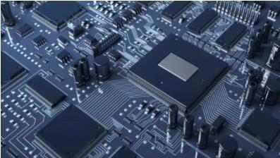
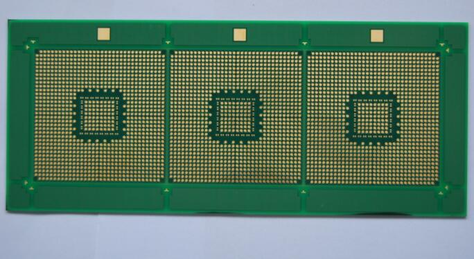
Wafer level chip packaging technology
WLCSP, also known as wafer level chip scale packaging technology in English, is different from the traditional chip packaging method (cutting and then sealing, and at least 20% of the volume of the original chip is increased after packaging). This latest technology is to package and test the whole wafer first, and then cut it into IC particles one by one, Therefore, the volume after packaging is equal to the original size of IC bare crystal. It is known as the future mainstream of packaging technology. Manufacturers that have been invested in R & D include FCT, Aptos, Casio, epic, Fujitsu, Mitsubishi electronics, etc.
It directly completes all operations on the wafer that ends the front-end wafer fabrication process. In the chip packaging process, the chip is separated from the wafer, so that WLCSP can achieve the minimum packaging volume with the same chip size, which is almost the final packaging miniaturization technology.
Wafer level chip scale packaging technology, integrating thin-film passive device technology and large-area specification manufacturing technology, not only provides cost saving solutions, but also provides shape factors consistent with the existing surface mount assembly process. Chip scale packaging technology not only provides a performance improvement roadmap, but also reduces the size of integrated passive devices.
Since the feasibility of WLCSP technology was announced in 1998, various types of WLCSP have appeared in the market in recent years. This technology has been used in mobile electronic devices, such as power supply chips for mobile phones, and extended to the application of logic products.
WLCSP is a variant of flip chip interconnection technology. With the help of WLCSP technology, the active surface of the bare chip is inverted and connected to the PCB with solder balls. The size of these solder balls is usually large enough (300 at 0.5mm spacing and pre reflow) μ m), the underfill process required for flip chip interconnection can be omitted

WLCSP Packaging
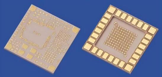
WLCSP can be divided into two structural types: direct bump and redistribution layer (RDL)
Direct bump
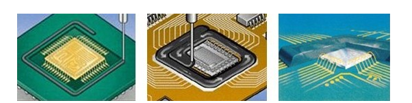
The direct bump WLCSP contains an optional organic layer (polyimide) that acts as a stress buffer on the surface of the active die. Polyimide covers the entire bare chip area except the windowed area around the connecting pad. A subbump metal layer (UBM) is sputtered or electroplated over this windowed area. UBM is a stack of different metal layers, including diffusion layer, barrier layer, wetting layer and oxidation resistance layer. The solder ball falls on the UBM (so called drop ball), and then the solder bump is formed by reflow welding.
Redistribution layer (RDL)
Redistribution layer (RDL) WLCSP this technology can convert bare chips designed for bonding lines (bonding pads are arranged around) into WLCSP. Unlike direct bumps, this WLCSP uses two polyimide layers. The first polyimide layer is deposited on the bare chip and keeps the bonding pad in the windowed state. The RDL layer converts the peripheral array into an area array by sputtering or electroplating. The subsequent structure is similar to a direct bump - including a second polyimide layer, UBM and a falling ball.
Advantages of WLCSP:
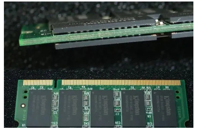
The packaging mode of WLCSP not only effectively reduces the size of memory module, but also meets the high-density requirements of mobile devices for body space; On the other hand, in terms of performance, it improves the speed and stability of data transmission. Standard SMT assembly equipment can be used without underfill process.
1. Minimum size of original chip packaging method:
The biggest feature of WLCSP wafer level chip packaging is to effectively reduce the package volume and make the package shape lighter and thinner. Therefore, it can be matched with mobile devices to meet the characteristic requirements of lightweight and short portable products.

Minimum size packaging
2. Short data transmission path and high stability:
When using WLCSP packaging, due to the short and thick circuit wiring (yellow line marked a to b), it can effectively increase the frequency of data transmission, reduce current consumption and improve the stability of data transmission. Due to the self calibration characteristics of light bare sheet in the welding process, the assembly yield is high.
3. Good heat dissipation characteristics
Because WLCSP has less traditional sealed plastic or ceramic packaging, the heat energy during IC chip operation can be effectively dissipated without increasing the temperature of the main body. This feature is of great help to the heat dissipation of mobile devices. It can reduce inductance and improve electrical performance.
WLCSP can not only realize the important technology of high-density and high-performance packaging and sip, but also play a key role in the device embedding PCB technology. Although the wire bonding process is very mature and flexible, the multi-layer circuit, fine line graphics and the combination with wire bonding of WLCSP technology show that it will have wider applications and new opportunities.
Disadvantages of WLCSP: the cost of WLCSP comes from wafer or packaging processing. If large-scale production is needed, the amount of labor needs to be increased. It will correspondingly increase the cost of production.
The future of WLCSP Technology
WLCSP has been applied in mobile phones, memory cards, car navigators and digital devices since it was applied in electronic watches in 2000. In the next few years, there will be more chips using WLCSP technology in the high-performance mobile market such as mobile phones.
The combination of WLCSP technology and chip embedding PCB process can ensure the stability of PCB assembly quality. This is because WLCSP is not only easy to mount PCB, but also has the characteristics of "known good die".
WLCSP technology brings more possibilities for the production of lightweight and compact electronic devices. WLCSP has been applied to circuit board assembly. Recently, it has also become an important part of SIP. MCP combining WLCSP and conventional wire bonding technology has also entered mass production.
Looking at the development of WLCSP in recent years, we can fully believe that WLCSP will continue to develop and expand to more fields in the near future.