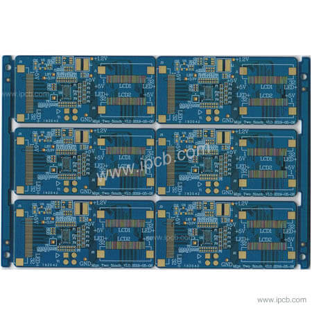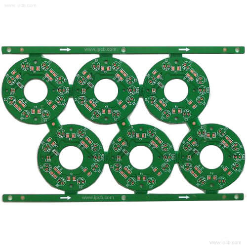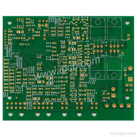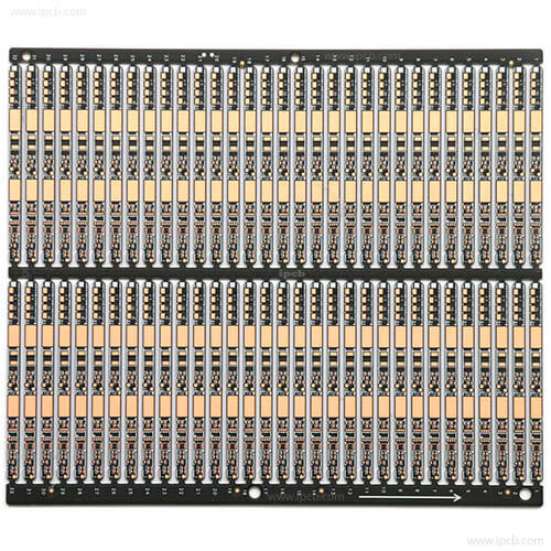
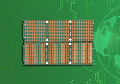

Model : Red solder mask + bonding gold finger pcb
Material : KB6160C
Layer : 2Layers
Color : Red/White
Finished Thickness : 1.2mm
Copper Thickness : 1OZ
Surface Treatment : immersion gold
Min Trace : 4mil(0.1mm)
Min Space : 4mil(0.1mm)
Special process : bonding pcb
PCB Board bonding is a way of wiring in the chip production process. It is generally used to connect the gold wire or aluminum wire of the internal circuit of the chip with the package pin or gold-plated copper foil of the circuit board before packaging. The ultrasonic wave from the ultrasonic generator (generally 40-140khz) is used, High frequency vibration is generated by the transducer and transmitted to the cleaver through the horn. When the cleaver contacts with the lead wire and the weldment, under the action of pressure and vibration, the surface of the metal to be welded rubs against each other, the oxide film is destroyed, and plastic deformation occurs, resulting in the close contact between two pure metal surfaces, achieving the combination of atomic distance, and finally forming a firm mechanical connection. Generally, after bonding (that is, after the circuit is connected to the pin), the chip is packaged with black glue.

PCB bonding method
BondingPCB process requirements
Process flow: cleaning PCB - dropping adhesive - chip bonding - bonding - sealing - testing
1. Clean PCB
The oil, dust and oxide layer on the bond location should be wiped with skin, and then the test position should be cleaned with a brush or blown with an air gun.
2. Drop adhesive
The amount of glue drop is moderate, the number of glue points is 4, and the four corners are evenly distributed; the bonding glue is strictly forbidden to pollute the pad.
3. Chip bonding (solid crystal)
Using vacuum suction pen, the suction nozzle must be flat to avoid scratching the wafer surface. Check the direction of the chip. When bonding to the PCBboard, it must be "stable and straight": flat, the wafer and PCB are parallel and tightly attached without virtual position; stable, the chip and PCB are not easy to fall off in the whole process; positive, the chip and PCB reserved position are directly attached, and can not be deflected. Pay attention to that the chip direction should not be reversed.
4. State line
The PCB of Bondin passed the Bondin pull test: 1.0 wire is greater than or equal to 3.5G, 1.25 wire is greater than or equal to 4.5g.
Standard aluminum wire with bonding melting point: the wire tail is greater than or equal to 0.3 times of wire diameter and less than or equal to 1.5 times of wire diameter.
The shape of aluminum wire solder joint is oval.
Solder joint length: greater than or equal to 1.5 times wire diameter, less than or equal to 5.0 times wire diameter.
Width of solder joint: greater than or equal to 1.2 times of wire diameter, less than or equal to 3.0 times of wire diameter.
During the bonding process, the operator should handle the wire with care, and the point should be accurately aligned. The operator should observe the bonding process with a microscope to see if there are defects such as broken state, winding, deviation, cold and hot welding, aluminum stripping, etc. if there is any, the relevant technical personnel must be informed to solve the problem in time.
Before the formal production, there must be a special person for the first time to check whether there are some defects, such as wrong state, missing state and so on. During the production process, special personnel shall be assigned to check its correctness regularly (at most 2 hours interval).
5. Sealing glue
Before sealing, check the regularity of the plastic ring before installing the plastic ring on the wafer to ensure that its center is square without obvious distortion. During the installation, ensure that the bottom of the plastic ring is close to the surface of the wafer, and there is no occlusion on the photosensitive area of the wafer center.
When dispensing, the black glue should completely cover the aluminum wire of the PCB solar cell and bonding chip, and can not expose the wire. The black glue can not seal out the PCBboard sun circle. The leakage should be removed in time. The black glue can not penetrate into the chip through the plastic ring.
In the process of glue dropping, the needle tip or the hairpin should not touch the wafer surface in the plastic ring and the bonding wire.
The drying temperature should be strictly controlled: the preheating temperature is 120 ± 5 degree Celsius, the time is 1.5-3.0 minutes; the drying temperature is 140 ± 5 degree Celsius and the time is 40-60 minutes.
After drying, there should be no air holes on the surface of the black glue. The height of the black glue should not be higher than the plastic ring.
6. Testing
Combination of various test methods:
A. Manual visual inspection
B. Quality inspection of bonder automatic welding line
C. Automatic optical image analysis (AOI) X-ray analysis to check the quality of inner solder joint
Model : Red solder mask + bonding gold finger pcb
Material : KB6160C
Layer : 2Layers
Color : Red/White
Finished Thickness : 1.2mm
Copper Thickness : 1OZ
Surface Treatment : immersion gold
Min Trace : 4mil(0.1mm)
Min Space : 4mil(0.1mm)
Special process : bonding pcb
For PCB technical problems, iPCB knowledgeable support team is here to help you with every step. You can also request PCB quotation here. Please contact E-mail sales@ipcb.com
We will respond very quickly.