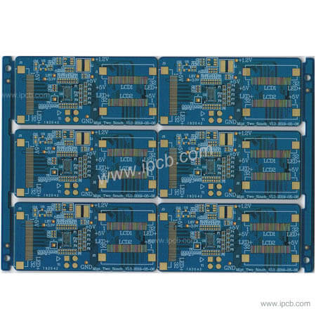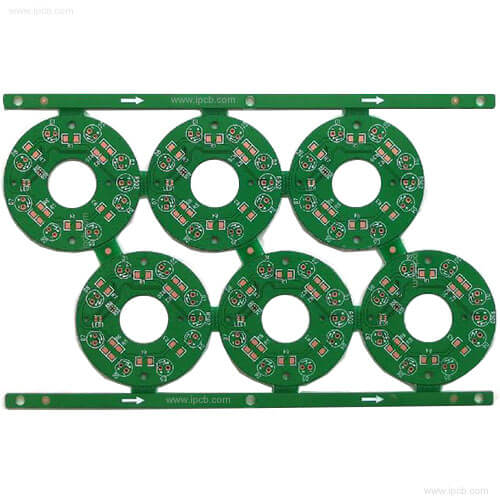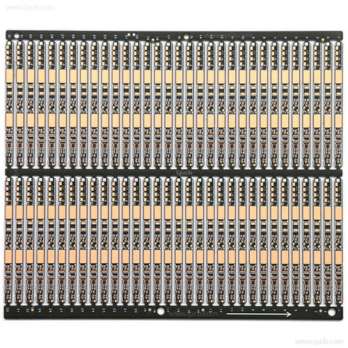

Model : Double side Power PCB
Material : FR4
Layer : 2Layers
Color : Green
Finished Thickness : 1.6mm
Copper Thickness : 1OZ
Surface Treatment : Free HASL pcb
Min Trace : 6mil(0.15mm)
Min Space : 6mil(0.15mm)
Application : Double side Power PCB
1. After the power supply comes in, it goes to the filter capacitor first. After it comes out of the filter capacitor, it is sent to the back equipment. Because the wiring on the PCB board is not an ideal wire, there is resistance and distributed inductance. If the power is taken from the front of the filter capacitor, the ripple will be relatively large, and the filtering effect will be poor. A kind of
2. The line should be paid attention to: if it is possible to make a wide line, it must not be thin, there must be no sharp chamfering, and no right angle should be used for turning. The ground wire should be as wide as possible. It is better to use a large area of copper coating. This docking point problem has been greatly improved. A kind of
3. Capacitors are set for switching devices (gate circuits) or other components that need filtering / decoupling. These capacitors should be arranged as close as possible to these components. If they are too far away, they will not work. When laying PCB (power board), what matters should be paid attention to in combination with safety regulations?
3.1. The minimum safety distance between the two wires before the fuse and that between the two wires and the enclosure or internal grounding of the AC power supply line shall not be less than 6 mm, and the minimum safety distance between the two wires and the enclosure or internal grounding shall not be less than 8 mm. A kind of
3.2 wiring requirements after fuse: the minimum creepage distance between zero and live wires shall not be less than 3mm. A kind of
3.3. The minimum creepage distance between high voltage area and low voltage area is not less than 8mm, less than 8mm or equal to 8mm. 2 mm safety slot must be opened.
4. The high-voltage area shall be provided with silk screen printing of high-voltage warning signs, i.e. triangle symbols including exclamation marks; the high-voltage area shall be framed with silk screen printing, and the frame bar silk screen printing shall not be less than 3mm
5. The minimum safe distance between positive and negative of high voltage rectifier filter is not less than 2mm. The design and development process are briefly described. A kind of
5.1. Make the schematic diagram according to the design
5.2 after the schematic diagram is compiled, the corresponding network table can be generated
5.3. Keep out layer
5.4 introduction of components and networks
5.5. Component layout the layout and routing of components have a great impact on the product life, stability and electromagnetic compatibility, which should be paid special attention to. Generally speaking, there should be some principles as follows: (1) placing sequence: first, place the components related to the structure in fixed position, such as power socket, indicator light, switch, connector and so on. After these devices are placed, they will be locked with the lock function of software, so that they will not be moved by mistake. Then place special components and large components on the circuit, such as heating elements, transformers, IC, etc. Finally, small devices are placed. (2) pay attention to heat dissipation and pay special attention to heat dissipation in the layout of components. For high-power circuits, those heating elements such as power tubes and transformers should be placed as far away as possible to facilitate heat dissipation. Do not concentrate in one place, nor high capacitance too close, so as to avoid premature aging of electrolyte.
6. Wiring
7. Adjustment and Perfection: after the wiring is completed, it is necessary to adjust the text, individual components, wiring and copper (this work should not be too early, otherwise it will affect the speed and bring trouble to the wiring), which is also for the convenience of production, debugging and maintenance. Copper coating usually refers to using large area copper foil to fill the blank area left after wiring. GND copper foil and VCC copper foil can be laid (but in case of short circuit, it is easy to burn the device, and it is better to ground it, unless it is used to increase the conduction area of power supply to bear large current before connecting VCC). Ground wrapping usually refers to wrapping a bunch of signal wires with special requirements by two ground wires (TRAC) to prevent it from being interfered or interfered by others. If copper is used instead of ground wire, attention must be paid to whether the whole ground is connected, the current size, flow direction and whether there are special requirements, so as to reduce unnecessary errors. A kind of
8. Checking and checking the network sometimes leads to the difference between the network relationship of the board drawn and the schematic diagram due to misoperation or negligence, so it is necessary to check the network. So after drawing, do not rush to the PCB manufacturer - ipcb.
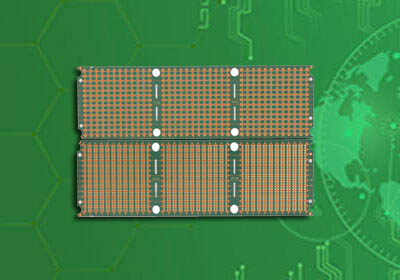
Model : Double side Power PCB
Material : FR4
Layer : 2Layers
Color : Green
Finished Thickness : 1.6mm
Copper Thickness : 1OZ
Surface Treatment : Free HASL pcb
Min Trace : 6mil(0.15mm)
Min Space : 6mil(0.15mm)
Application : Double side Power PCB
For PCB technical problems, iPCB knowledgeable support team is here to help you with every step. You can also request PCB quotation here. Please contact E-mail sales@ipcb.com
We will respond very quickly.