")
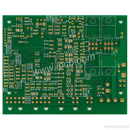
Model : Double-side Printed Circuit Board (PCB)
Material : KB-6160C
Layer : 2Layers
Color : Green/White
Substrate copper thickness : 1OZ
Finished copper thickness : 1.5OZ
Finished Thickness : 1.6mm
Surface Treatment : Immersion gold(ENIG)
Application : Consumer Electronics
This is a mass production Double-side Printed Circuit Board (PCB) that is maturely produced by ipcb. We provide customers with low-cost PCBs and allow customers' products to occupy the market.
Double-sided Printed Circuit Board (PCB) is a very important type of PCB. There are double-sided circuit board metal base Printed Circuit Board (PCB) on the market, Hi-Tg heavy copper foil Printed Circuit Board (PCB), flat winding High-frequency double-sided Printed Circuit Board (PCB), high-frequency Printed Circuit Board (PCB), hybrid dielectric base high-frequency double-sided Printed Circuit Board (PCB), etc. It is suitable for a wide range of high-tech industries such as: telecommunications, power supply, Computers, industrial control, digital products, scientific and educational equipment, medical equipment, automobiles, aerospace, etc.
Double-sided PCB Craft
Double-sided Printed Circuit Board (PCB) is usually made of epoxy glass cloth copper clad board. It is mainly used for communication electronic equipment, advanced instruments and electronic computers with high performance requirements.
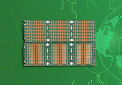
The production process of Double-sided Printed Circuit Board (PCB) is generally divided into process wire method, hole blocking method, masking method and pattern plating-etching method. The process flow of pattern plating-etching method is shown in the figure.
 production process")
Printed Circuit Board (PCB) production process
Double-sided PCB Proofing
Double-sided Printed Circuit Board (PCB) proofing, the most commonly used is craftsmanship. At the same time, rosin process, OSP process, gold plating process, immersion gold and silver plating processes are also applicable in Double-sided Printed Circuit Board (PCB).
Spray tin process: good appearance, the pad is silver-white, the pad is easy to tin, solder is easy, and the price is low.
Sikkim process: stable quality, usually used in the case of bonding IC.
The difference between a double-sided PCB and single-sided PCB
The difference between a double-sided Printed Circuit Board (PCB) and a single-sided Printed Circuit Board (PCB) is that the circuit of the single-sided Printed Circuit Board (PCB) is only on one side of the PCB, while the double-sided Printed Circuit Board (PCB) The circuit can be on both sides of the PCB board, with vias in the middle to connect the double-sided PCB circuit.
Parameters of Double-sided Printed Circuit Board (PCB) The production of double-sided Printed Circuit Board (PCB) is different from that of single-sided Printed Circuit Board (PCB). In addition to the production process, there is also an additional copper sinking process, that is, double-sided The process of circuit conduction.
Model : Double-side Printed Circuit Board (PCB)
Material : KB-6160C
Layer : 2Layers
Color : Green/White
Substrate copper thickness : 1OZ
Finished copper thickness : 1.5OZ
Finished Thickness : 1.6mm
Surface Treatment : Immersion gold(ENIG)
Application : Consumer Electronics
For PCB technical problems, iPCB knowledgeable support team is here to help you with every step. You can also request PCB quotation here. Please contact E-mail sales@ipcb.com
We will respond very quickly.