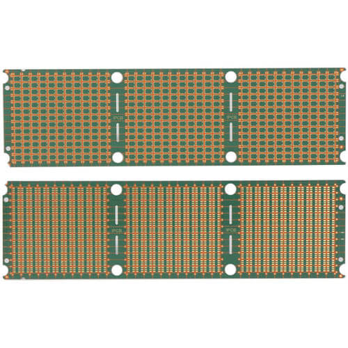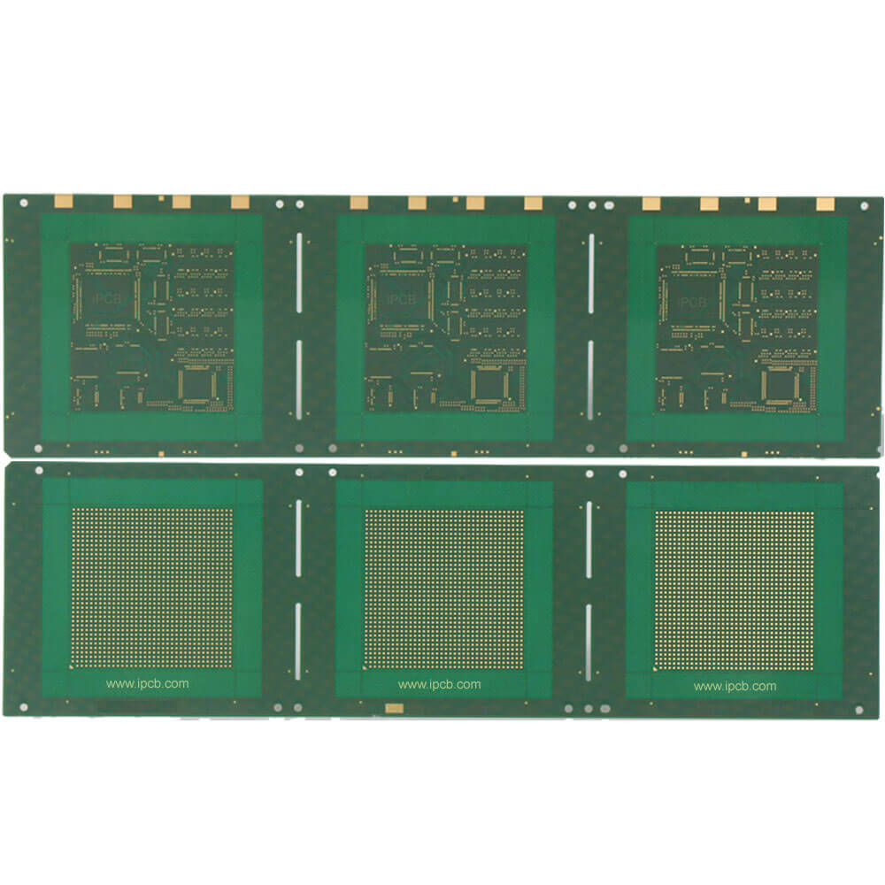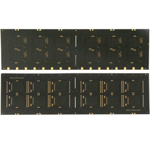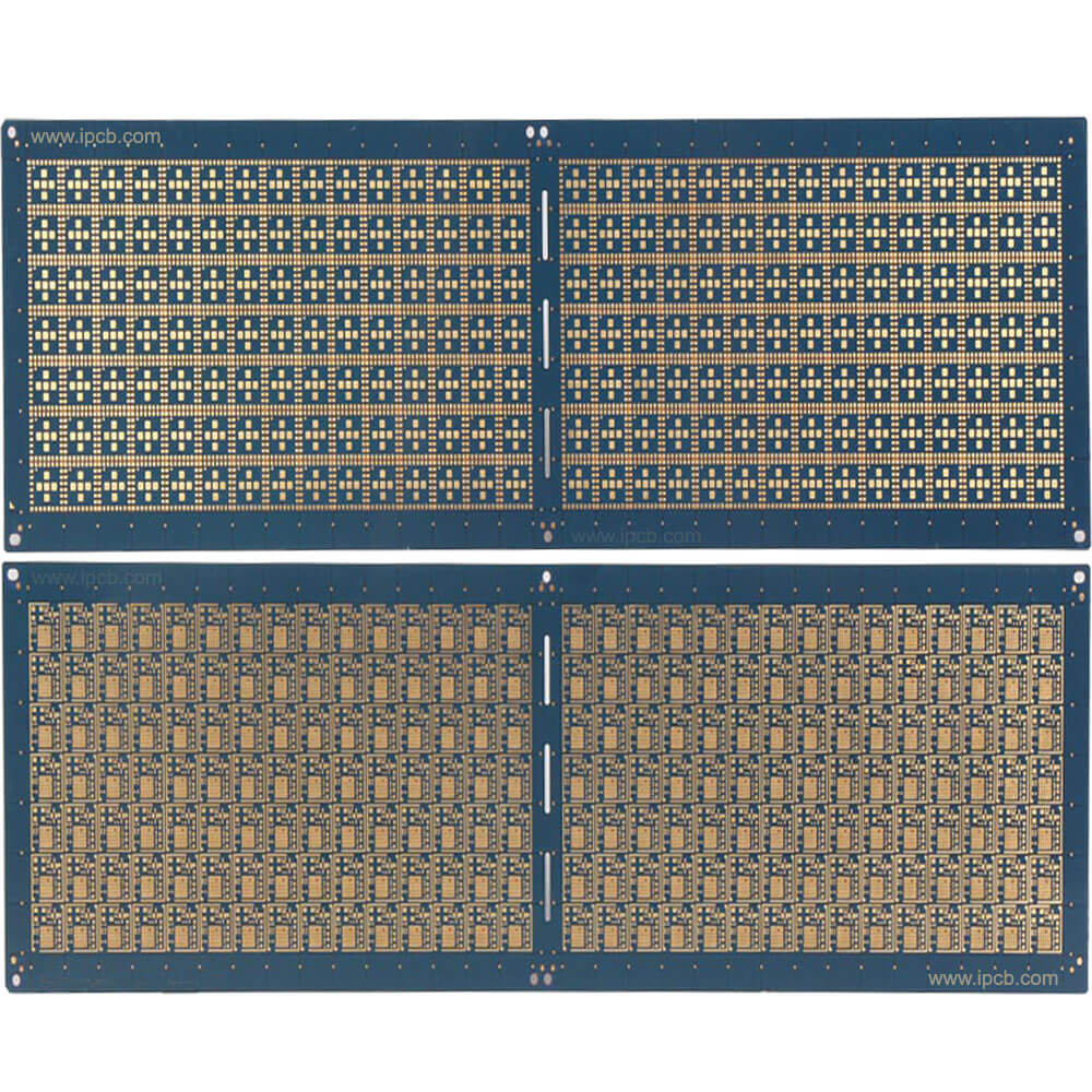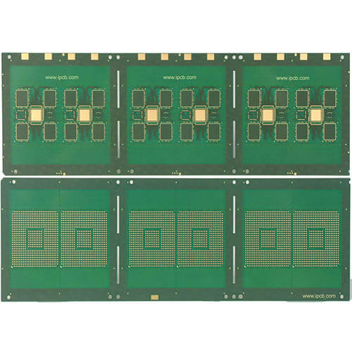
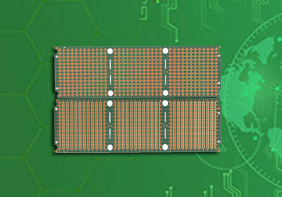

Product Name: BGA IC substrate
Plate: Mitsubishi Gas HF BT HL832NX-A-HS
Minimum width / spacing: 30 / 30um
Surface: ENEPIG(2U)
PCB thickness: 0.3mm
Layer: 4Layers
Structure: 1L-4L,1L-2L,3L-4L
Solder mask ink: TAIYO PSR4000 AUS308
Aperture: Laser hole 0.075mm, Mechanical hole 0.1mm
Application: BGA IC substrate
BGA IC Substrate framework refers to a kind of key special basic material used for IC Substrate. It is mainly used to protect the chip and act as the interface between the IC chip and the outside world. Its form is ribbon, usually golden. The specific use process is as follows: first, the IC Substrate is pasted on the IC Substrate frame by the fully automatic mounter, then the contacts on the IC chip and the nodes on the IC Substrate frame are connected by the wire bonding machine to realize the circuit connection, and finally the IC chip is protected by the packaging material to form the IC Substrate, which is convenient for later application. The supply of IC Substrate framework depends on import.
TAIYO PSR4000 AUS308 is a special ink for IC Substrate. It is easy to lose oil in the pre-treatment of super coarsening and Zonghua. The ink is delicate. The pre-treatment adopts sandblasting + Super coarsening. The nickel palladium process does not lose oil. The color is very beautiful. The copper surface must be cleaned. The roughness is not very important. The adhesion is good. Sandblasting must be used to minimize the difference of copper surface, Parameters of plug hole plate: 75 degree Celsius for 1 hour, 95 degree Celsius for 1 hour, 110 degree Celsius for 1 hour, then 150 degree Celsius for 50 minutes, baking for 25 minutes after printing text, horizontal drying section after text, 180 degrees. Note: the effect of pozzolanic is worse than sandblasting. It doesn't need to be too hard to eliminate the difference between local copper surface and local copper surface. Just like the color difference of gold surface, it only needs a little bit of sandblasting. The emery can be a little thicker, 280 mesh.
BGA (Ball Grid Array)-ball pin grid array packaging technology, high-density surface mount packaging technology. At the bottom of the package, the pins are spherical and arranged in a grid-like pattern, hence the name BGA. Motherboard control chipsets mostly use this type of packaging technology, and the material is mostly ceramic. The memory packaged with BGA technology can increase the memory capacity by two to three times without changing the volume of the memory. Compared with TSOP, BGA has a smaller volume, better heat dissipation performance and electrical performance. BGA packaging technology has greatly improved the storage capacity per square inch. With the same capacity, memory products using BGA packaging technology are only one-third of the volume of TSOP packaging; compared with traditional TSOP packaging, BGA packaging has A faster and more effective way to dissipate heat.
The I/O terminals of the BGA package are distributed under the package in the form of circular or columnar solder joints. The advantage of BGA technology is that although the number of I/O pins has increased, the pin spacing has not decreased but increased. Improves the assembly yield; although its power consumption increases, BGA can be welded with a controlled collapse chip method, which can improve its electrothermal performance; thickness and weight are reduced compared with previous packaging technology; parasitic parameters are reduced, The signal transmission delay is small, and the frequency of use is greatly improved; the assembly can be coplanar welding, and the reliability is high.
BGA (Ball Grid Array) package, that is, ball grid array package, is to make array solder balls on the bottom of the package body substrate as the I/O end of the circuit to interconnect with the printed circuit board (PCB). The device packaged with this technology is a surface mount device. Compared with traditional foot-mounted devices (LeadedDe~ce such as QFP, PLCC, etc.), BGA packaged devices have the following characteristics.
1) There are many I/Os. The number of I/Os of a BGA packaged device is mainly determined by the size of the package body and the pitch of the solder balls. Since the solder balls of the BGA package are arranged in an array under the package substrate, the number of I/Os of the device can be greatly increased, the size of the package body can be reduced, and the space occupied by assembly can be saved. Generally, with the same number of leads, the package size can be reduced by more than 30%. For example: CBGA-49, BGA-320 (pitch 1.27mm) compared with PLCC-44 (pitch 1.27mm) and MOFP-304 (pitch 0.8mm), the package size is reduced respectively 84% and 47%.
2) Improve the placement yield and potentially reduce the cost. The lead pins of traditional QFP and PLCC devices are evenly distributed around the package body, and the pitch of the lead pins is 1.27mm, 1.0mm, 0.8mm, 0.65mm, 0.5mm. As the number of I/Os increases, the pitch must become smaller and smaller. When the pitch is less than 0.4mm, the accuracy of the SMT equipment is difficult to meet the requirements. In addition, the lead pins are extremely easy to deform, which leads to an increase in placement failure rate. The solder balls of the BGA devices are arranged in an array at the bottom of the substrate, which can be arranged with a larger number of I/Os. The standard solder ball pitch is 1.5mm, 1.27mm, 1.0mm, and the fine pitch BGA (printed BGA, also known as CSP-BGA, when the pitch of the solder balls is less than 1.0mm, it can be classified as CSP package) pitches are 0.8mm, 0.65mm, 0.5mm, and the current Some SMT process equipment is compatible, and its placement failure rate is less than 10ppm.
3) The contact surface between the BGA array solder balls and the substrate is large and short, which is good for heat dissipation.
4) The pins of the BGA array solder balls are very short, which shortens the signal transmission path and reduces the lead inductance and resistance, thus improving the performance of the circuit.
5) The coplanarity of the I/O end is obviously improved, and the loss caused by the poor coplanarity during the assembly process is greatly reduced.
6) BGA is suitable for MCM packaging and can realize the high density and high performance of MCM.
7) BGA and ~BGA are both firmer and more reliable than ICs with fine pitch footprint packages.
Product Name: BGA IC substrate
Plate: Mitsubishi Gas HF BT HL832NX-A-HS
Minimum width / spacing: 30 / 30um
Surface: ENEPIG(2U)
PCB thickness: 0.3mm
Layer: 4Layers
Structure: 1L-4L,1L-2L,3L-4L
Solder mask ink: TAIYO PSR4000 AUS308
Aperture: Laser hole 0.075mm, Mechanical hole 0.1mm
Application: BGA IC substrate
For PCB technical problems, iPCB knowledgeable support team is here to help you with every step. You can also request PCB quotation here. Please contact E-mail sales@ipcb.com
We will respond very quickly.