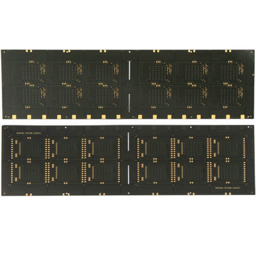
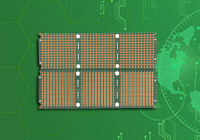

Model: HDI IC Substrate Board
Material: SI10U
Layers: 6L(2+2+2)
Thickness: 0.6mm
Single size: 35 * 35mm
Resistance welding: PSR-4000 AUS308
Surface treatment: ENEPIG
Minimum aperture: 0.1mm
Minimum line distance: 70um
Minimum line width: 30um
Application: HDI IC Substrate Board
Features of SI10U(S)
. Low CTE and high modulus, which can effectively reduce the warpage of the package carrier
. Excellent heat and humidity resistance
. Good PCB processability
. Halogen-free materials
Application field
eMMC, DRAM
AP, PA
Dual CM
Fingerprint, RF Module
SI10U IC package substrate PCB board parameter specification
| Item | Condition | Unit | SI10U(S) |
|---|---|---|---|
| Tg | DMA | degree Celsius | 280 |
| Td | 5% wt. loss | degree Celsius | >400 |
| CTE (X/Y-axis) | Before Tg | ppm/ degree Celsius | 10 |
| CTE (Z-axis) | α1/α2 | ppm/ degree Celsius | 25/135 |
| Dielectric Constant 1) (1GHz) | 2.5.5.9 | - | 4.4 |
| Dissipation Factor 1) (1GHz) | 2.5.5.9 | - | 0.007 |
| Peel Strength1) | 1/3 OZ, VLP Cu | N/mm | 0.80 |
| Solder Dipping | @288 degree Celsius | min | >30 |
| Young's modulus | 50 degree Celsius | GPa | 26 |
| Young's modulus | 200 degree Celsius | GPa | 23 |
| Flexural Modulus1) | 50 degree Celsius | GPa | 32 |
| Flexural Modulus1) | 200 degree Celsius | GPa | 27 |
| Water Absorption1) | A | % | 0.14 |
| Water Absorption1) | 85 degree Celsius/85%RH,168Hr | % | 0.35 |
| Flammability | UL-94 | Rating | V-0 |
| Thermal Conductivity | - | W/(m.K) | 0.61 |
| Color | - | - | Black |
IC carrier board packaging frame refers to a key special basic material used for IC card module packaging. It mainly protects the chip and serves as the interface between the integrated circuit chip and the outside world. Its form is ribbon, usually golden yellow . The specific usage process is as follows: First, the IC card chip is attached to the IC card packaging frame by a fully automatic placement machine, and then the contacts on the IC chip are connected to the nodes on the IC card packaging frame with a wire bonding machine. The connection of the circuit, and finally the use of packaging materials to protect the integrated circuit chip to form an integrated circuit card module, which is convenient for subsequent applications.
The IC carrier board is also a product based on the BGA (Ball Grid Array, ball-planting matrix array or ball-planting array) architecture. The manufacturing process is similar to that of PCB products, but the precision is greatly improved. The manufacturing process is different from PCB. IC substrate has become a key component in IC packaging, gradually replacing part of the lead frame (Lead Frame) application.
An integrated circuit integrates a general-purpose circuit on a chip. It is a whole. Once it is damaged internally, the chip is also damaged. The PCB can solder the components by itself, and replace the components if it is broken.
IC carrier board: generally the carrier board on the chip, the board is very small, usually the size of a 1/4 fingernail, the board is very thin 0.2~0.4mm, the material used is FR-5, BT resin, and the circuit is 2mil/ About 2mil. It is a high-precision board that used to be generally produced in Taiwan, but now it is trending towards the mainland. The industry's yield rate is 75%. The unit price of this kind of board is very high, generally buy according to PCS.
Model: HDI IC Substrate Board
Material: SI10U
Layers: 6L(2+2+2)
Thickness: 0.6mm
Single size: 35 * 35mm
Resistance welding: PSR-4000 AUS308
Surface treatment: ENEPIG
Minimum aperture: 0.1mm
Minimum line distance: 70um
Minimum line width: 30um
Application: HDI IC Substrate Board
For PCB technical problems, iPCB knowledgeable support team is here to help you with every step. You can also request PCB quotation here. Please contact E-mail sales@ipcb.com
We will respond very quickly.