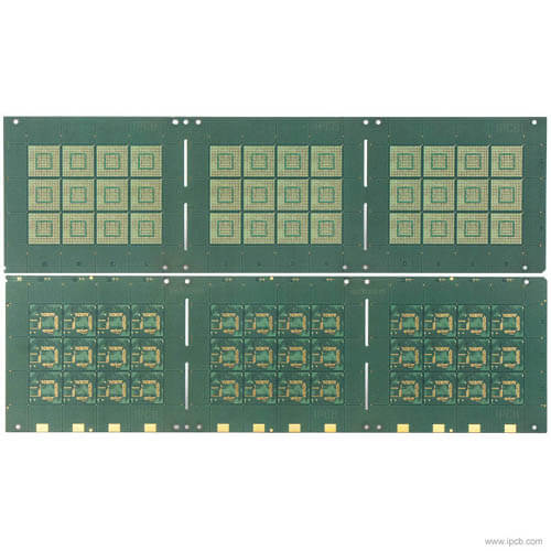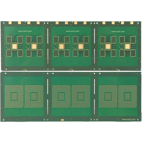
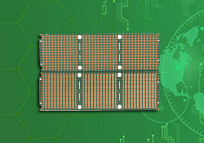

Model: LGA package IC substrate
Material: SI165
Layers: 4L
Thickness: 0.4mm
Single size: 8 * 8mm
Resistance welding: PSR-2000 BL500
Surface treatment: ENEPIG
Minimum aperture: 0.1mm
Minimum line distance: 100um
Minimum line width: 40um
Application: LGA package IC substrate
The full name of LGA package is Land Grid Array package, which literally translates to grid array packaging, which corresponds to the previous packaging technology of Intel processors, Socket 478, which is also called Socket T. Said it is a "leapfrog technological revolution", mainly because it replaces the previous pin-shaped pins with metal contact packaging. The LGA775, as the name suggests, has 775 contacts.
Because the pins become contacts, the installation method of the processor with the LGA775 interface is also different from that of the current product. It cannot use the pins to fix the contact, but needs a mounting bracket to fix it, so that the CPU can be pressed correctly. On the elastic tentacles exposed by the Socket, the principle is the same as the BGA package, except that the BGA is soldered to death, and the LGA can be unlocked at any time to replace the chip. The "B (Ball)" in BGA-tin bead, the chip and the motherboard circuit are contacted by the tin bead, this is the BGA package.

More and more high-density, multi-function and miniaturization requirements have brought new challenges to packaging and substrates, and many new packaging technologies have emerged, including buried packaging technologies. Embedded packaging technology is to embed passive components such as resistors, capacitors, inductors, and even active components such as ICs into the printed circuit board. This approach can shorten the line length between components, improve electrical characteristics, and improve The effective printed circuit board packaging area reduces a large number of solder joints on the printed circuit board surface, thereby improving the reliability of the packaging and reducing the cost. It is a very ideal high-density packaging technology.
Early embedded technology was mainly applied to PCBs, and now it is also applied to package substrates. Embedding passive components such as resistors and capacitors in PCBs is already a very mature technology, and iPCB has mastered this type of technology for a long time. The transfer of buried technology from the PCB to the substrate is more difficult to achieve. Because the substrate has higher precision and thinner breakdown thickness, it requires stronger manufacturing and processing capabilities and higher precision. However, because the technical principle is the same, the passive devices embedded in the substrate also quickly achieved mass production.
IPCB has two main types of passive components such as resistors and capacitors embedded in the substrate. One is planar burying, also called thin-film burying, which means that only a few microns of resistors and capacitors are embedded in the board and transferred through graphics., Acid etching and other series of processes to make corresponding resistance or capacitance patterns. The other method is discrete embedding, which is to put the resistors and capacitors of ultra-thin package specifications such as 01005, 0201, 0402 directly into the substrate through the SMT process and the hole-filling interconnection process. Buried packaging does not limit the number of components embedded. It mainly depends on the packaging area. If the area is sufficient, more can be buried. Although the packaging cost of this approach will become higher, the cost of the entire product may not become higher, because the subsequent component purchase and SMT chip cost can be saved, and the performance will also be improved.
In addition to embedding passive components such as resistors, capacitors, and inductors, ipcb circuits are also actively developing embedded IC technology, that is, directly embedding the chip die into the substrate for board-level packaging, which is more complicated than embedding passive components . After long-term technology accumulation and innovation, ipcb circuit company has now produced IC embedded substrate samples. The next step is to jointly develop with customers and define the final product according to their needs. The ipcb circuit is now mainly looking for customers who have ideas in this area to jointly develop and make productization and engineering. We already have the technology, but we need to apply this technology to products on a large scale in the follow-up and improve the production yield and reliability. We also need to look for customers who are willing to do this, and find some real products to do it.
The demand for high-density, miniaturized packaging is increasing, and the market for built-in component substrates is expected to continue to expand. The emergence of embedded technology contains the possibility of major changes in the industrial structure and industry structure, from material factories, IC foundries, IC design companies to printed circuit board/substrate manufacturers, packaging manufacturers, system manufacturers, that is, upstream and downstream of the industry chain The collaboration is indispensable. The development of embedded technology has a great impact on the original device suppliers, and they need to change at this time. For example, his devices need to meet the embedded conditions. The emergence of new technologies will definitely break the inherent pattern. It is very important for enterprises to keep abreast of market changes and make timely transformation. "
As SoC chip integration is close to the physical limit, advanced packaging technologies such as wafer-level packaging (CSP), system-in-package (SiP), and device embedding provide a feasible way for further system integration. At present, leading complete machine equipment manufacturers not only consider device functions when designing products, but also start to consider packaging design, module design, embedded PCB design, etc., and are actively looking for innovative component and module packaging solutions to improve the system Reliability, reduce product size, realize product optimization and innovation.
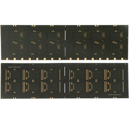
Model: LGA package IC substrate
Material: SI165
Layers: 4L
Thickness: 0.4mm
Single size: 8 * 8mm
Resistance welding: PSR-2000 BL500
Surface treatment: ENEPIG
Minimum aperture: 0.1mm
Minimum line distance: 100um
Minimum line width: 40um
Application: LGA package IC substrate
For PCB technical problems, iPCB knowledgeable support team is here to help you with every step. You can also request PCB quotation here. Please contact E-mail sales@ipcb.com
We will respond very quickly.