

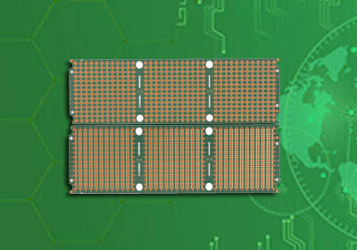

Model: Fingerprint card IC package substrate
Material: Shengyi SI10U
Layers: 2L
Thickness: 0.2mm
Single size: 11 * 11mm
Resistance welding: PSR-4000 AUS308
Surface treatment: Soft Gold+Hard Gold
Minimum aperture: 0.1mm
Minimum line distance: 75um
Minimum line width: 35um
Application: Fingerprint card IC package substrate
SI10U IC package substrate PCB board parameter specification
| Item | Condition | Unit | SI10U(S) |
|---|---|---|---|
| Tg | DMA | degree Celsius | 280 |
| Td | 5% wt. loss | degree Celsius | >400 |
| CTE (X/Y-axis) | Before Tg | ppm/ degree Celsius | 10 |
| CTE (Z-axis) | α1/α2 | ppm/ degree Celsius | 25/135 |
| Dielectric Constant 1) (1GHz) | 2.5.5.9 | - | 4.4 |
| Dissipation Factor 1) (1GHz) | 2.5.5.9 | - | 0.007 |
| Peel Strength1) | 1/3 OZ, VLP Cu | N/mm | 0.80 |
| Solder Dipping | @288 degree Celsius | min | >30 |
| Young's modulus | 50 degree Celsius | GPa | 26 |
| Young's modulus | 200 degree Celsius | GPa | 23 |
| Flexural Modulus1) | 50 degree Celsius | GPa | 32 |
| Flexural Modulus1) | 200 degree Celsius | GPa | 27 |
| Water Absorption1) | A | % | 0.14 |
| Water Absorption1) | 85 degree Celsius/85%RH,168Hr | % | 0.35 |
| Flammability | UL-94 | Rating | V-0 |
| Thermal Conductivity | - | W/(m.K) | 0.61 |
| Color | - | - | Black |
Traditional IC package substrate uses a lead frame as an IC conducting circuit and a carrier supporting the IC, and it connects the pins on both sides or around the lead frame. With the development of IC package technology, the number of pins has increased, the wiring density has increased, and the number of substrate layers has increased. Traditional package forms cannot meet the needs of the market. In recent years, new IC package forms represented by BGA and CSP have emerged, and a new carrier for semiconductor chip package, an IC package substrate, has also emerged.
In the early stage of the IC package substrate market, Japan preemptively occupied most of the market share. Later, the package substrate industry in South Korea and Taiwan began to rise and develop rapidly, and gradually formed a "three pillars" with Japan to carve up most of the world's package substrate markets. Japan, Taiwan, and South Korea are still the most important supply regions for IC package substrates in the world. Japanese IC package substrate manufacturers are well-known companies such as Ibiden, Shinko, Kyocera, and Eastern; while Korean manufacturers are mainly SEMCO, Simmteck, and Daeduck. ; The famous ones in Taiwan are UMTC, Nanya, Kinsus and ASEM.
In terms of technology, Japanese manufacturers are still relatively advanced. However, in recent years, Taiwanese manufacturers have gradually opened up their production capacity, and they have more cost advantages in more mature products (such as PBGA), sales volume has continued to rise, and rapid growth. According to statistics from the market research organization Prismark in 2012, Taiwanese companies accounted for four of the top 11 substrate companies in the world in terms of sales revenue.
According to iPCB Circuit Company, iPCB Circuit Company has the mass production capacity of PBGA, WB-CSP, passive device embedding and other IC package substrate, and can provide FC-BGA, FC-CSP, FC-POP, FC-SiP and other IC package substrate samples. Current substrate products include BGA, Camera, SiP, Memory, MEMS, RF substrates, etc.

IC package substrate PCB board
The trend of IC package substrate is thinning and miniaturization, requiring finer line spacing and smaller apertures. This poses higher challenges for material selection, surface coating technology, fine line production, and fine solder mask processing. iPCB Circuit Company is also constantly catching up with more advanced package substrate technology. At present, the iPCB has mass-produced substrate line width/line distance up to 35/35µm, blind hole/aperture minimum of 75/175µm, and through hole/aperture 100/ 230μm, solder resist alignment accuracy ±35μm, etc., and the surface coating material adopts E'lyTIc Ni/Au, ENEPIG, OSP, AFOP. By next year, these parameters will be upgraded to achieve line width/line spacing 20/20µm, blind holes/rings as small as 65/150µm, through holes/aperture 100/200µm, solder mask alignment accuracy ±20µm, and surface coating New materials such as Immersion TIn will be used for the cover.
As the electronic industry develops faster and faster, new products are emerging one after another, and the requirements for upstream chips and package are getting higher and higher. SiP package technology has the advantages of miniaturization, high performance, multi-function integration, etc., which can realize the integrated package of multiple chips, which can greatly save product volume and improve reliability requirements, and thus has received extensive attention from the industry. In order to meet the industry's increasing demand for SiP package, iPCB combines its own business capabilities and the upstream and downstream of the industry chain to provide one-stop services from SiP design, PCB/substrate production, soldering processing, sample package, and testing.
The user only needs to hand over the package design requirements to iPCB at the beginning of the tape-out, and the SiP package samples can be obtained about one week after the tape-out. iPCB's SiP design includes device modeling and die stacking design, package substrate design, embedded active chip substrate design, and embedded passive device substrate design. Based on the multi-structure experimental platform, that is, the package experimental line is the main platform, and the three auxiliary platforms for failure analysis, environmental reliability testing, and signal function testing, iPCB has formed the key capability layout of SiP package technology research and development, and expanded the product type to QFN and BGA, LGA, POP, PiP, SiP, 3D embedded and other packages. "
The iPCB Circuit R&D Management Department stated that most of the customers that iPCB substrate business faced before were package manufacture r, but with the changes in the industry trend, the strategy is now gradually adjusted, and it is more oriented towards chip manufacturers and terminal system manufacturers. Directly facing the package factory is more proactive and has a stronger grasp, because the chip design, package design, PCB design, etc. must be considered when making product definitions. System manufacturers or chip manufacturers want to use the lowest cost and the most reasonable way to make products, but also need back-end companies like iPCB circuits to cooperate.
For chip or system manufacturers, iPCB must rely on advanced package technology if they want to innovate. Our company is the company with the most complete resource integration in back-end manufacturing. We have the ability to do substrates, PCBs, PCBA, and IC package substrates, which can help them achieve innovation in products. There is also a trend in the future that the entire semiconductor industry is slowly merging and cooperating with each other, not as clear as the original division. iPCB provides a one-stop service, considering that if you do package alone or substrate alone, you will eventually become nowhere because it is difficult to achieve breakthroughs without new things. Only by fusing these things together and infiltrating each other, Integrate new technologies, then these technologies will bring new experiences and new competitiveness.
Model: Fingerprint card IC package substrate
Material: Shengyi SI10U
Layers: 2L
Thickness: 0.2mm
Single size: 11 * 11mm
Resistance welding: PSR-4000 AUS308
Surface treatment: Soft Gold+Hard Gold
Minimum aperture: 0.1mm
Minimum line distance: 75um
Minimum line width: 35um
Application: Fingerprint card IC package substrate
For PCB technical problems, iPCB knowledgeable support team is here to help you with every step. You can also request PCB quotation here. Please contact E-mail sales@ipcb.com
We will respond very quickly.


