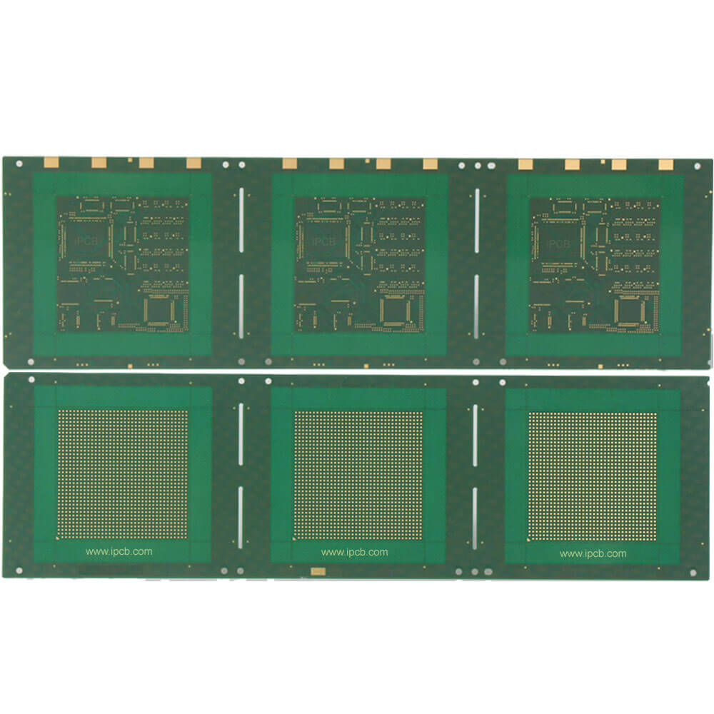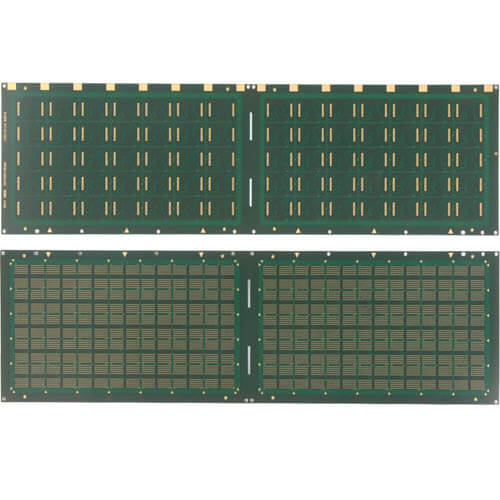

Model: USB 3.0 PCB Substrate Board
Material: SI10U
Layers: 4L
Thickness: 0.3mm
Single size: 12.8 * 38.8mm
Resistance welding: PSR-2000 BL500
Surface treatment: Soft Gold
Minimum aperture: 0.1mm
Minimum line distance: 75um
Minimum line width: 40um
Application: USB 3.0 PCB Substrate Board
USB 3.0 can provide up to 5Gbps data rate, ten times faster than high-speed USB (USB 2.0), and has optimized power efficiency. At these high transmission rates, signal integrity issues are becoming more and more restrictive on PCB traces and wiring lengths, as well as design and implementation functions. Poor signal quality may seriously affect system performance and reliability. The USB 3.0 ReDriver Superspeed in terminal applications is a dual-channel (TX± and RX±), single-channel USB3.0 redriver, used in terminal applications such as notebook computers, desktops, docking stations, backplanes and wiring. Each channel provides selectable equalization settings to compensate for different input wiring losses.

USB3.0 PCB design summary
Reasonable layout design:
The USB controller and the USB connector should be as close as possible to reduce the length of the trace. The magnetic beads and decoupling capacitors used for decoupling and removing high-frequency noise interference should be placed as close to the USB connector as possible.
The terminal device matching resistor should be placed as close as possible to the end of the USB controller.
The voltage regulator should also be placed as close as possible to the connector.
Wiring design:
Minimize the length of the trace, give priority to the wiring of the high-speed USB differential line, and try to prevent the high-speed USB differential line and any connectors and digital signal lines with steep edges from approaching the wiring.
Try to reduce the number of vias and corners on the USB high-speed signal line, so as to ensure the control of characteristic impedance and prevent signal reflection.
It is strictly forbidden to use a 90° routing angle, use two forty-five degrees to achieve a turn or use an arc to achieve it, which will greatly reduce the signal reflection and the non-continuity of the characteristic impedance.
Do not run signal lines under crystal oscillator circuits, crystals, clock synthesizers, ICs with magnetic components and clock memory overclocking.
Prevent short stubs from appearing on the signal line, otherwise it may cause signal reflections and affect signal integrity. If short stubbing is unavoidable, make sure that its length does not exceed 50 mils.
Try to put high-speed signal lines in the same layer. Ensure that the return path of the trace has a detailed mirror plane (VCC or GND, first select the GND plane) without segmentation. If possible, do not extend the trace beyond the dividing line of the mirror plane (such as the dividing line of a different switching power supply on the switching power supply plane), otherwise it may increase the self-inductance and expand the signal radiation.
Differential signal lines are wired together side by side.
Differential signal routing
The wiring spacing between the parallel USB differential signal pairs must ensure a differential characteristic impedance of 90 ohms.
Reduce the length of the high-speed USB signal line, high-speed clock line and AC signal side by side, or increase the spacing between them, thereby reducing the impact of crosstalk. Ensure that the distance between the differential pair signal and other signal traces is at least 50 mils.
The tight coupling mode is selected for the differential pair signal, that is, the spacing between the traces is lower than the total width of the trace, so that the ability of the differential signal to resist external noise interference can be improved. The actual trace spacing and total width must be calculated based on the relevant mobile phone software.
Differential signal is best to ensure that the distance between the two traces is consistent everywhere, and to ensure that the length is matched, the larger length difference (such as the length difference between DP and DM) cannot exceed 50 mils.
Length matching is more critical than keeping the spacing consistent everywhere. Therefore, priority is given to ensuring length matching. Signal traces can be routed where the trace spacing cannot be kept consistent to ensure that the lengths of the two traces are consistent.
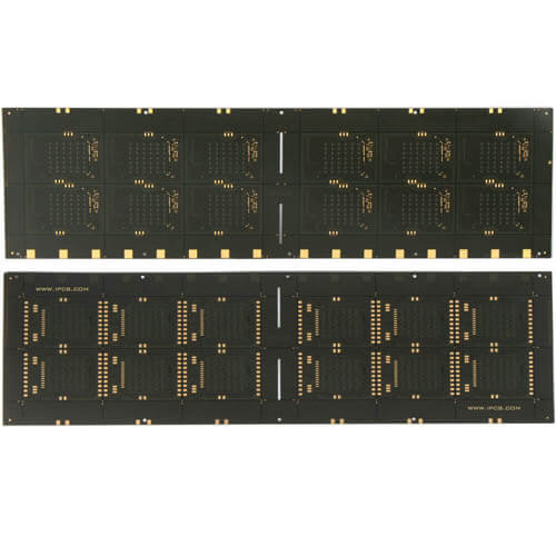
Model: USB 3.0 PCB Substrate Board
Material: SI10U
Layers: 4L
Thickness: 0.3mm
Single size: 12.8 * 38.8mm
Resistance welding: PSR-2000 BL500
Surface treatment: Soft Gold
Minimum aperture: 0.1mm
Minimum line distance: 75um
Minimum line width: 40um
Application: USB 3.0 PCB Substrate Board
For PCB technical problems, iPCB knowledgeable support team is here to help you with every step. You can also request PCB quotation here. Please contact E-mail sales@ipcb.com
We will respond very quickly.