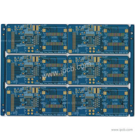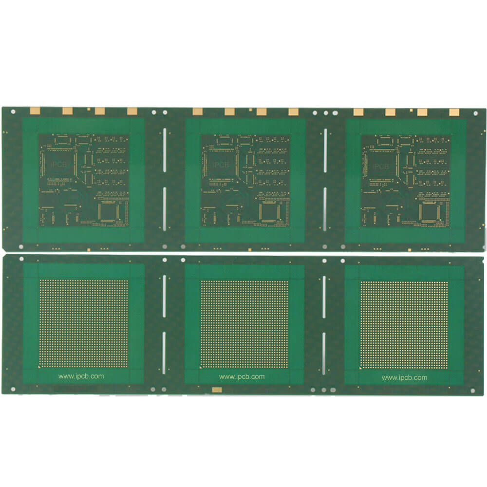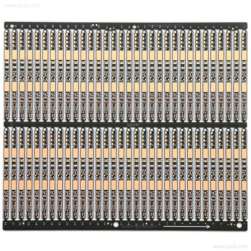

Model: Blind vias IC Substrate
Material: Mitsubishi Gas HF BT HL832NX
Layers: 8layers
Thickness: 0.6mm
Single size: 40 * 55mm
Resistance welding: PSR-4000 AUS308
Surface treatment: soft gold
Minimum aperture: 0.1mm
Minimum line distance: 30um
Minimum line width: 30um
Application: Blind vias IC Substrate
In blind vias IC substrate proofing, the application of blind holes and buried holes greatly reduces the size and quality of blind vias IC substrate PCB, reduces the number of layers, improves electromagnetic compatibility, increases the characteristics of electronic products, reduces costs, and makes the design work more simple and fast.
Blind vias: blind vias are vias that connect the inner wiring of PCB with the surface wiring of PCB. This hole does not penetrate the whole board.
Buried vias: buried vias only connect the via type of wiring between the inner layers, so they can't be seen from the PCB surface.

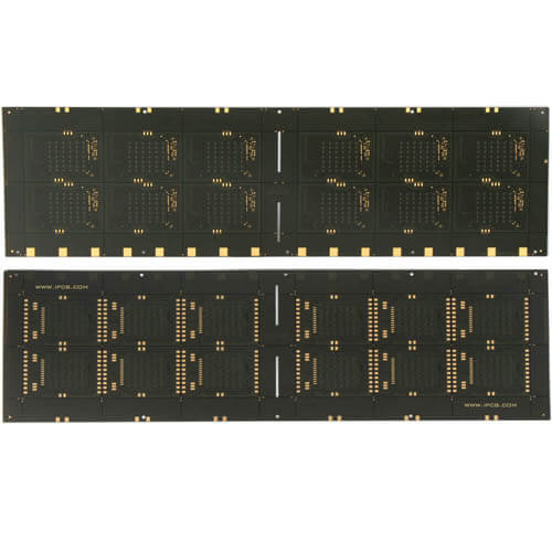
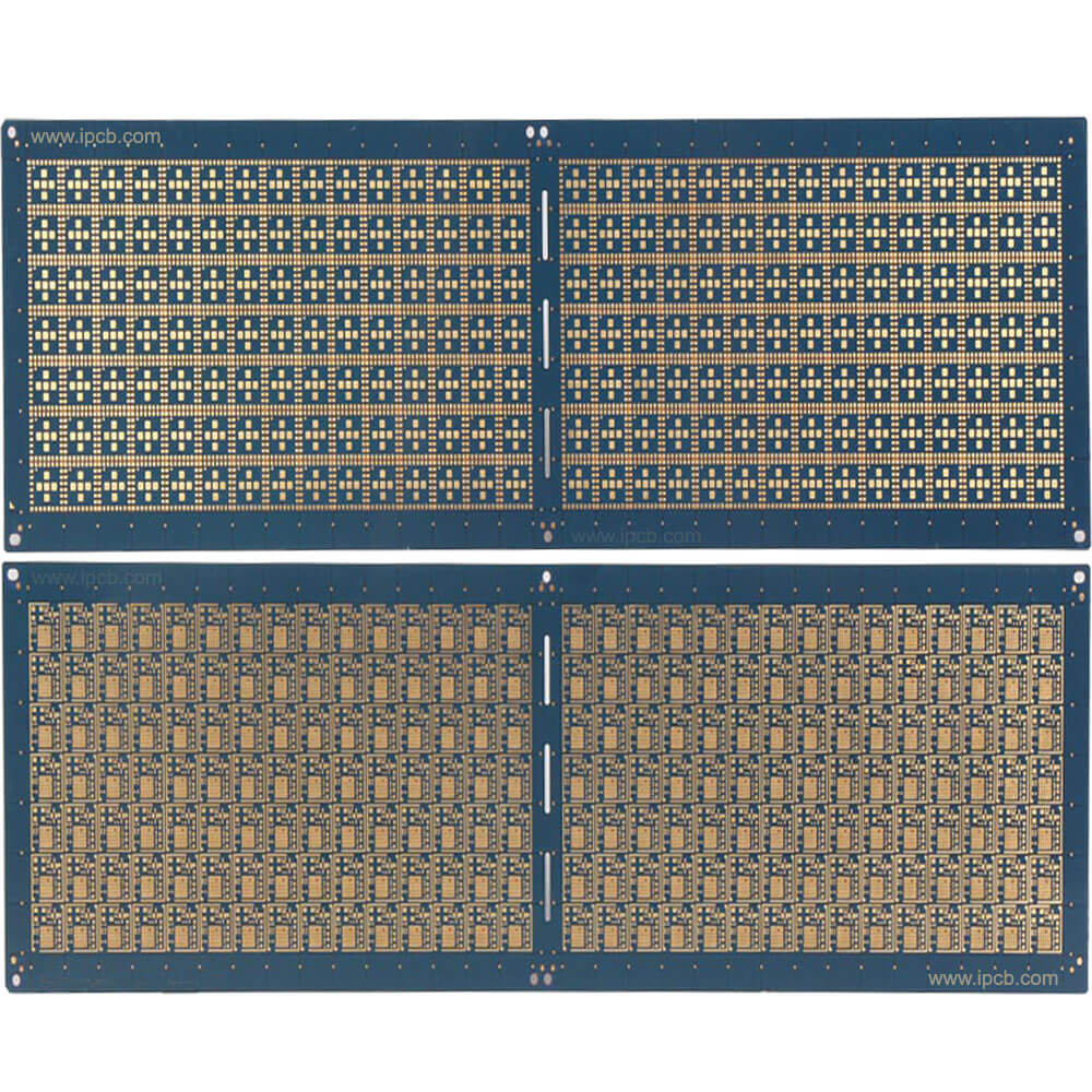
Blind vias IC Substrate
From the beginning of the 20th century to the beginning of the 21st century, the PCB board industry has developed by leaps and bounds in technology, and the electronic assembly technology has been rapidly improved. As a printed PCB board industry, IPCB can only be developed synchronously with it.
Can continue to meet the needs of customers. With the small, light and thin electronic products, printed PCB board have developed flexible boards, rigid-flex boards, buried/blind via IC Substrate multilayer boards and so on.
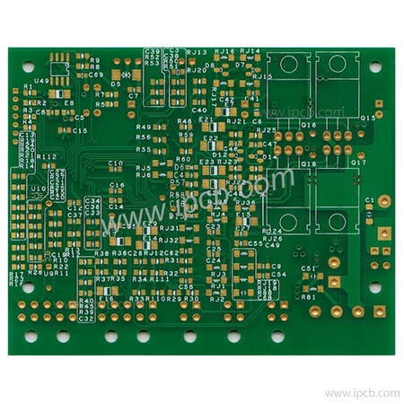
Speaking of blind/buried vias, first we start with the traditional multilayer board. The structure of the standard multi-layer PCB board contains inner and outer circuits, and then uses drilling and metallization processes in the holes to achieve the internal connection function of each layer of circuits. However, because of the increase in circuit density, the packaging methods of parts are constantly updated. In order to allow the limited PCB board area to place more high-performance parts, in addition to the thinner circuit width, the diameter of the hole has also been reduced from 1 mm in the DIP jack to 0.6 mm in the SMD, and further reduced to 0.4mm and 0.3mm, Below 0.2mm. However, it still occupies the surface area, so there will be buried vias and blind vias IC Substrate.
The most effective way to increase PCB density is to reduce the number of through holes, and accurately set blind holes and buried holes. Blind vias IC Substrate manufacturing is very difficult. The production process of this kind of Blind vias IC Substrate board can assess the overall process level, design ability, experience and wisdom of an IC Substrate PCB factory.
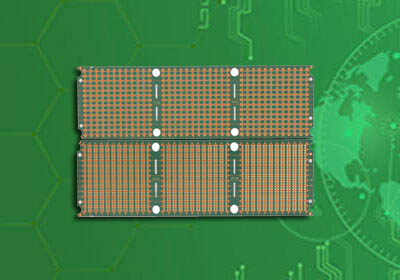
Model: Blind vias IC Substrate
Material: Mitsubishi Gas HF BT HL832NX
Layers: 8layers
Thickness: 0.6mm
Single size: 40 * 55mm
Resistance welding: PSR-4000 AUS308
Surface treatment: soft gold
Minimum aperture: 0.1mm
Minimum line distance: 30um
Minimum line width: 30um
Application: Blind vias IC Substrate
For PCB technical problems, iPCB knowledgeable support team is here to help you with every step. You can also request PCB quotation here. Please contact E-mail sales@ipcb.com
We will respond very quickly.