Il substrato di imballaggio è il costo più grande diImballaggio IC, accounting for more than 30%.Imballaggio IC i costi includono substrati di imballaggio, packaging materials, ammortamento e collaudo delle apparecchiature, among which the cost ofSchede portanti IC accounted for more than 30%. It is the largest cost of integrated circuit packaging and occupies an important position in integrated circuit packaging. Per IC carrier boards, the substrato materials include copper foil, substrate, dry film (solid photoresist), wet film (liquid photoresist) and metal materials (copper balls, nickel beads, and gold salts), of which the substrate accounts for The ratio exceeds 30%, which is the largest cost end ofSchede portanti IC.
(1 )One of the main raw materials: copper foil
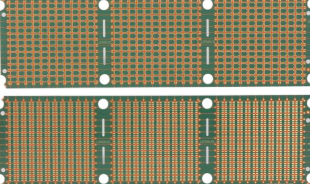
Similar to PCB, Il foglio di rame richiesto per il bordo portante IC è anche foglio di rame elettrolitico, and it needs to be ultra-thin uniform copper foil, the thickness can be as low as 1.5μm, generalmente 2-18μm, while the thickness of copper foil used in traditional PCB is 18, Circa 35¼m. The price of ultra-thin copper foil is higher than that of ordinary electrolytic copper foil, and it is more difficult to process.
(2) The second of the main raw materials: substrate plate
The substrate of the carrier board is similar to the copper clad laminate of the PCB, che è diviso principalmente in tre tipi: substrato duro, flexible film substrate and co-fired ceramic substrate. Tra loro, hard substrate and flexible substrate have more room for development, mentre lo sviluppo del substrato ceramico co-bruciato tende a rallentare.
The main considerations for IC carrier substrates include dimensional stability, caratteristiche ad alta frequenza, heat resistance and thermal conductivity and other requirements:

Attualmente, ci sono principalmente tre materiali per substrati rigidi di imballaggio, vale a dire materiale BT, materiale ABF e materiale MIS;
Flexible packaging substrate substrate materials mainly include PI (polyimide) and PE (polyester) resin;
Ceramic packaging substrate materials are mainly ceramic materials such as alumina, aluminum nitride, and silicon carbide.
Rigid substrate materials: BT, ABF, MIS
(1) BT resin
The full name of BT resin is "bismaleimide triazine resin", which was developed by Mitsubishi Gas Company of Japan. Although the patent period of BT resin has expired, Mitsubishi Gas Company è ancora leader nello sviluppo e nell'applicazione della resina BT. BT resin has many advantages such as high Tg, elevata resistenza al calore, moisture resistance, low dielectric constant (Dk) and low dissipation factor (Df), but due to the glass fiber layer, è più duro del substrato FC fatto di ABF. The wiring is more troublesome, and the difficulty of laser drilling is higher, which cannot meet the requirements of fine lines, but it can stabilize the size and prevent thermal expansion and contraction from affecting the line yield. Therefore, BT materials are mostly used for networks with high reliability requirements. Chip and programmable logic chip. At present, I substrati BT sono principalmente utilizzati in prodotti quali chip MEMS del telefono cellulare, communication chips, e chip di memoria. With the rapid development of LED chips, the application of BT substrates in LED chip packaging is also developing rapidly.
(2) ABF
ABF material is a material led by Intel and used for the production of high-end carrier boards such as Flip Chip. Rispetto al materiale base BT, ABF material can be used as IC with thinner circuit, suitable for high pin count and high transmission, and is mostly used for large high-end chips such as CPU, GPU e chipset. As a build-up material, ABF può essere utilizzato come circuito collegando direttamente ABF sul substrato della lamina di rame, and there is no need for a thermocompression bonding process. In the past, ABFFC had the problem of thickness. Tuttavia, as the technology of copper foil substrates is becoming more and more advanced, ABFFC può risolvere il problema dello spessore finché viene utilizzato il piatto sottile. In the early days, Le schede carrier ABF sono state utilizzate principalmente per le CPU nei computer e nelle console di gioco. With the rise of smart phones and changes in packaging technology, L'industria ABF è scesa in un basso ebb, but in recent years, Le velocità di rete sono aumentate e le innovazioni tecnologiche hanno portato sul tavolo nuove applicazioni di calcolo ad alte prestazioni. The ABF demand is magnified again. Dal punto di vista delle tendenze del settore, ABF substrates can keep up with the pace of advanced semiconductor manufacturing processes and meet the requirements of fine lines and fine line width/spaziatura tra linee. The future market growth potential can be expected. Con capacità produttiva limitata, industry leaders have begun to expand production. A maggio 2019, Xinxing announced that it expects to invest 20 billion yuan from 2019 to 2022 to expand high-end IC flip-chip substrate factories and vigorously develop ABF substrates. In termini di altri produttori taiwanesi, Jingsus expects to shift the production of similar substrates to ABF, e Nandian sta anche continuando ad aumentare la capacità produttiva.
(3) MIS
MIS substrate packaging technology is a new type of technology that is currently developing rapidly in the analog, IC di potenza, and digital currency markets. MIS è diverso dai substrati tradizionali in quanto contiene uno o più strati di strutture preincapsulate, and each layer is interconnected by electroplating copper to provide electrical connections during the packaging process. MIS può sostituire alcuni pacchetti tradizionali come pacchetti QFN o pacchetti basati su frame lead perché MIS ha funzionalità di cablaggio più fini, better electrical and thermal properties, e un profilo più piccolo.
Flexible substrate materials: PI, PE

PI and PE resins are widely used in flexible PCBs andSchede portanti IC, especially in tapeSchede portanti IC. I substrati flessibili del film sono principalmente suddivisi in substrati adesivi a tre strati e substrati senza adesivi a due strati. The three-layer rubber sheet was originally mainly used for military electronic products such as launch vehicles, missili da crociera, and space satellites, e successivamente ampliato a vari chip di prodotto elettronici civili; lo spessore del foglio senza gomma è più piccolo, suitable for high-density wiring, ed è resistente al calore. , Thinning and thinning have obvious advantages. I prodotti sono ampiamente utilizzati nell'elettronica di consumo, elettronica automobilistica e altri settori, which are the main development directions for flexible packaging substrates in the future.
Ci sono molti produttori di materiali substrati a monte, and the domestic technology is relatively weak.
Ci sono molti tipi di substrati di materiale centrale per IC carrier boards, and most upstream manufacturers are foreign-funded enterprises. Prendi come esempio i materiali BT e ABF più utilizzati. The main global hard substrate manufacturers are Japanese companies MGC and Hitachi Korean companies Doosan and LG. I materiali ABF sono prodotti principalmente dal giapponese Ajinomoto, and the country has just started.