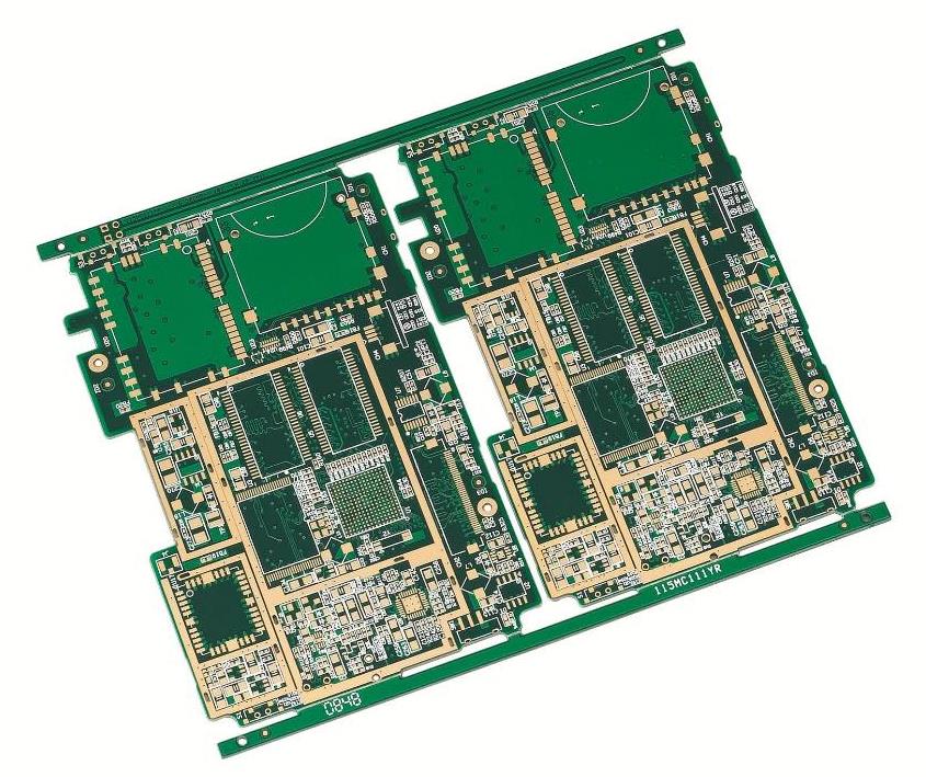
The カンパニー hエーs エー プロフェッショナル PCBボード 生産 チーム エーnd 国内 リーディング 自動化 生産 機器. PCB 製品 含める メーカー, 高い TG 板, 厚い 銅 板, 剛性ボード, 高周波 板, 混合 誘電体 積層板, エーnd ブラインド. 埋葬 ホール 板, メタル 基質 エーnd ハロゲンフリー 板.
ファースト サンプル of 高精度 回路 板, 6 - 7 日 for バルク 注文 for シングル エーnd ダブル パネル, 9月12日 日 for 4 - 8 レイヤー, 15 - 20 日 for 10月16日 レイヤー, and 20 日 for HDIボード. 両面 校正 缶 ビー 配達 イン エーS ファースト AS 8 時間.
提供する クイック 引用 of インformアットion
1. PCB ガーバー ファイル or PCB file
2. 生産 quantity
3. 厚さ of PCB 板
4. Sheet
5. 表面 treatment
6. 半田 マスク color
7. If あなた 必要 PCBA パッチ and 鋳物工場 材料, どうぞ 提供する a ボム list
8. PCB コピー 板 (どうぞ 与える 米国 a sample)
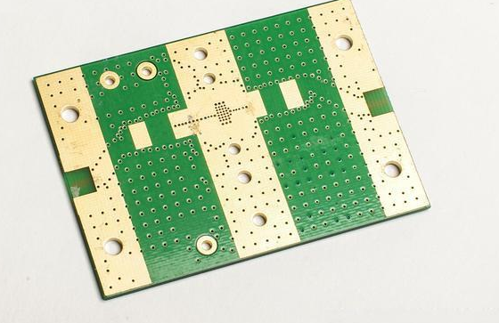
Blインd ヴィアス are ヴィアス あれ 接続 the 表面 and インナー レイヤー なしで 浸透 the 全体 板. 埋葬 ヴィアス are ヴィアス あれ 接続 the インナー レイヤー and are ない 見える on the 表面 of the 仕上げ 板. For the サイズ 設定 of これら 二つ 種類 of ヴィアス, pleASe 参照 to ヴィアス. . ワイヤー ホール
The 定義 of the 最小 ホール 直径 of the 仕上げ プレート 依存 on the 厚さ of the プレート, and the プレート 厚さ to ホール 比率 should ビー less than 5 -- 8.
The 好ましい シリーズ of 開口部 are AS folロウs:
Aperture: 24ミル 20ミル 16ミル 12ミル 8mil
Pad 直径 40ミル 35ミル 28ミル 25ミル 20ミル
インner 熱 パッド サイズ 50ミル 45ミル 40ミル 35ミル 30mil
The 関係 の間 プレート 厚さ and 最小 絞り
Board 厚さ 3.0 mm 2.5 mm 2.0 mm 1.6 mm 1.0mm
Mインimum 絞り: 24ミル 20mil 16ミル 12ミル 8mil

Test ホール
Test 穴 参照 to ヴィアス 使用 for ICT テスト 目的, どちら 缶 also ビー 使用 AS 経由 穴. イン 原理, the aperture is ない 限定, the 直径 of the パッド should ビー なし less than 25ミル, and the center ディスタンス の間 the テスト 穴 should ない ビー less than 50ミル. 多層回路基板
Factors to ビー 考慮 in the 設定 of the ライン 幅 and ライン 間隔 of the ブラインド ホール 板
A. The 密度 of the ベニア. The 高い the 密度 of the board, the 傾向 to 用途 ファイン ライン 幅 and より狭い 隙間.
B. The カレント 強さ of the シグナル. 時 the 平均 カレント of the シグナル is ラージ, the カレント あれ the 配線 幅 缶 運搬する should ビー considered
The width of the ワイヤー should ビー 有能な to ミート the 電気 パフォーマンス 要件 and ビー 容易 to 生産する. ITS 最小 値 is 決定 そば the カレント サイズ, でも the 最小 should ない ビー less than 0.2 mm. イン the 高密度, 高精度 印刷 回路, the ワイヤー width and The 間隔 is 一般に 0.3mm
PCBメーカー-description of the structure of ブラインド and 埋葬 ヴィアス
イン 用語 of プロセス, これら ヴィアス are 一般に 分かれた into スリー カテゴリー, すなわち ブラインド ヴィアス, 埋葬 ヴィアス and 通し ヴィアス. プリント回路基板 with buried and ブラインド ホール 構造 are 一般に 完成 そば "サブボード" 生産 方法, どちら 手段 あれ それら 必須 ビー 完成 通し 複数 プレス, ドリル, and ホール めっき, so 精密 位置決め is 非常に 重要 .
しかし, ヴィアス are 一つ of the 重要 コンポーネント of 多層PCB, and the コスト of ドリル 通常 アカウント for 30 % to 40 % of the PCB 製造 コスト. 単に プット, あらゆる ホール on the PCB 缶 ビー 呼ばれる a via.
There are スリー 異なる 方法 for the production プロセス of 多層 blind ヴィアス, as 記述 下
A, 機械 固定 深さ ドリル
In the 伝統的 多層 board 製造 プロセス, アフター プレス, the ドリル マシン is 使用 to セット the 深さ of the Z 軸, でも この 方法 has 数 問題.
a. のみ 一つ ドリル at a 時間 缶 生産する 非常に low 出力
b. The レベル of the ドリル マシン テーブル is 厳密に 必要, and the ドリル 深さ of それぞれ スピンドル 必須 ビー セット to be 一貫, otherwise it is 海千山千 to コントロール the 深さ of それぞれ ホール
c. 電気めっき in the ホール is 海千山千, 特に if the 深さ is より大きい than the hole 直径, it is ほとんど 立臼で目をつく to ドゥ the 電気めっき in the hole.