
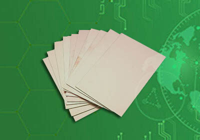
F4B-1/2 Teflon PCB glass fabric copper-clad laminates is laminated with excellent material according to the requirements of microwave circuit in electrical performance. It is a kind of laminate of microwave PCB due to its excellent electrical performance and higher mechanical strength.
F4B-1/2 Teflon PCB Technical Specifications
Appearance | Meet the specification requirements for the laminate of microwave PCB by National and Military Standards. | |||||||||||||||||
Types | F4B255 | F4B265 | ||||||||||||||||
Dielectric Constant | 2.55 | 2.65 | ||||||||||||||||
Dimension(mm) | 300*250 380*350 440*550 500*500 460*610 600*500 840*840 1200*1000 1500*1000 | |||||||||||||||||
For special dimension,customized laminates is available. | ||||||||||||||||||
Copper thickness | 0.035μm,0.018μm | |||||||||||||||||
Thickness and Tolerance(mm) | Laminate thickness | 0.17, 0.25 | 0.5, 0.8, 1.0 | 1.5, 2.0 | 3.0, 4.0, 5.0 | |||||||||||||
Tolerance | ±0.025 | ±0.05 | ±0.05 | ±0.09 | ||||||||||||||
The laminate thickness includes the copper thickness. For special dimension,customized laminates is available. | ||||||||||||||||||
Mechanical Strength | Warp | Thickness(mm) | Maximum Warp | |||||||||||||||
Original board | Single side | Double side | ||||||||||||||||
0.25~0.5 | 0.030 | 0.050 | 0.025 | |||||||||||||||
0.8~1.0 | 0.025 | 0.030 | 0.020 | |||||||||||||||
1.5~2.0 | 0.020 | 0.025 | 0.015 | |||||||||||||||
3.0~5.0 | 0.015 | 0.020 | 0.010 | |||||||||||||||
Cutting/punching Strength | Thickness1mm,no burrs after cutting,minimum space between two punching holes is 0.55mm,no delamination. | |||||||||||||||||
Thickness1mm,no burrs after cutting,minimum space between two punching holes is 1.10mm,no delamination. | ||||||||||||||||||
Peel strength(1oz copper) | Normal state:≥15N/cm;No bubble, delamination, peel strength≥12N/cm(in the constant humidity and temperature, and keep in the melting solder of 260 degree Celsius±2 degree Celsius for 20 seconds). | |||||||||||||||||
Chemical Property | According to the properties of laminate,the chemical etching method for PCB can be used. The dielectric properties of laminate are not changed. The plating through hole can be done,but the sodium treatment or the plasma treatment must be used. | |||||||||||||||||
Electrical Property | Name | Test condition | Unit | Value | ||||||||||||||
Density | Normal state | g/ cm3 | 2.2~2.3 | |||||||||||||||
Moisture Absorption | Dip in the distilled water of 20±2 degree Celsius for24 hours | % | ≤0.1 | |||||||||||||||
Operating Temperature | High-low temperature chamber | degree Celsius | -50 degree Celsius~+260 degree Celsius | |||||||||||||||
Thermal Conductivity | W/m/k | 0.3 | ||||||||||||||||
CTE (typical) | 0~100 degree Celsius | ppm/ degree Celsius | 16(x) | |||||||||||||||
21(y) | ||||||||||||||||||
186(z) | ||||||||||||||||||
Shrinkage Factor | 2 hours in boiling water | % | 0.0002 | |||||||||||||||
Surface Resistivity | 500V DC | Normal state | M·Ω | ≥1*104 | ||||||||||||||
Constant humidity and temperature | ≥5*103 | |||||||||||||||||
Volume Resistivity | Normal state | MΩ.cm | ≥1*106 | |||||||||||||||
Constant humidity and temperature | ≥9*104 | |||||||||||||||||
Pin Resistance | 500VDC | Normal state | MΩ | ≥5*104 | ||||||||||||||
Constant humidity and temperature | ≥5*102 | |||||||||||||||||
Surface dielectric strength | Normal state | d=1mm(Kv/mm) | ≥1.2 | |||||||||||||||
Constant humidity and temperature | ≥1.1 | |||||||||||||||||
Dielectric Constant | 10GHZ | εr | 2.55,2.65 (±2%) | |||||||||||||||
Dissipation Factor | 10GHZ | tgδ | ≤1*10-3 | |||||||||||||||

iPCB.com Products:
Radio/Microwave/Hybrid High Frequency, FR4 Double/Multi-Layer, 1~3+N+3 HDI,Anylayer HDI, Rigid-Flex, Blind Buried, Blind Slot, Backdrilled, IC,Heavy Copper Board and etc.
*Any question,Don't hesitate to contact us through www.ipcb.com, We will get back to you as soon as possible.
*Send inquiry to sales@ipcb.com


