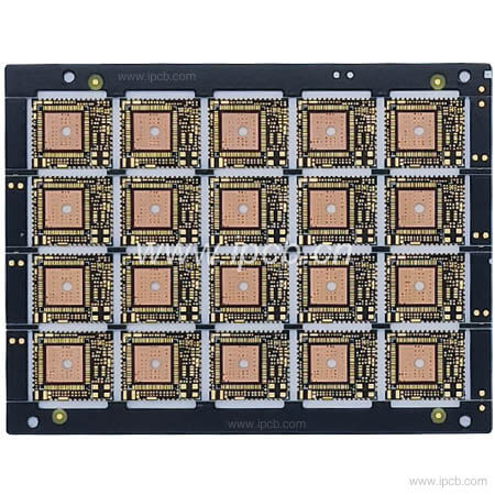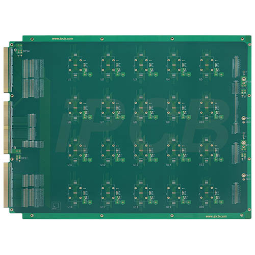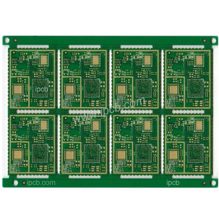
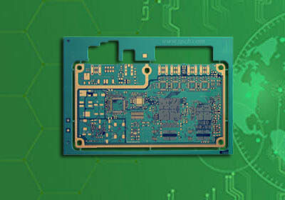

Model : Multilayer vehicle wifi module pcb
Material : FR4
Layer : 6Layers
Color : Green/White
Finished Thickness : 1.0mm
Copper Thickness : 1OZ
Surface Treatment : Immersion Gold
Min Trace : 3mil(0.75mm)
Min Space : 3mil(0.75mm)
characteristic : Half hole PCB
Application : WiFi Bluetooth Module pcb
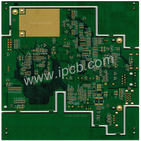
PCB design requirements of vehicle mounted products
Design concept:
In the design stage of circuit and PCB, it is necessary to combine with the production process to avoid the non-standard design and increase the processing difficulty and cost. The most important thing is that if the PCB needs to be redesigned or changed greatly, the reliability tests conducted in this trial production are meaningless and can not reflect the production requirements of the final product
Design requirements:
1. Each component must be provided with detailed specifications. During circuit design, it is necessary to check whether the device meets the requirements of vehicle regulations and whether there are lead-free models. During PCB design, it is necessary to check whether the welding temperature curve meets the production requirements. If it can not meet the requirements, the pad size and component packaging shall be in accordance with the component manufacturer's recommendations Size to do, to avoid non-standard design caused by processing difficulties;
2. The pad size of SMR resistor and capacitor should be increased on the basis of the standard. For the specific size, please refer to the document requirements. The purpose is to ensure sufficient welding, higher requirements on the car, and avoid desoldering and false soldering caused by long-term vibration
3. The vias and pads of plug-in components shall be designed in accordance with the manufacturer's specification. If there is no relevant content in the specification, the manufacturer shall be required to provide a written reference size
4. If the chip aluminum electrolytic capacitor is placed on the side of reflow soldering only once, the aluminum electrolysis will be damaged if reflow twice
5. Gap between components of reflow soldering process: ≥ 0.4mm, calculated by the outermost dimension
6. The gap between the plug-in element and the patch element: ≥ 3mm, which is convenient for manual repair welding or local reflow soldering
7. Large and heavy components should be placed on the side of reflow soldering only once to prevent falling off and false soldering caused by secondary reflow soldering
8. Components cannot be placed within 5mm of the processing edge, and test points cannot be placed within 3mm. Wiring can be done, but white glaze for protection should be coated on the wiring line to avoid scratching during processing
9. The highest range of component height should be determined according to the processing machine (Mounter / reflow welder) to avoid components too high to be processed
10. The components within 10-20 mm near the welding side shall be placed separately as far as possible to avoid insufficient welding due to too dense components
11. Components with large size should not be close to each other, which will cause inconvenience in repair and uneven heat in reflow soldering will cause poor welding
12. The plug-in components should be placed on the same side as far as possible to facilitate processing
13. Elements with polarity (aluminum capacitor / tantalum capacitor / diode, etc.) shall be arranged in the same direction as far as possible, so as to facilitate visual inspection. If it cannot be placed in this way due to performance considerations, it must also be locally aligned
14. The tag number of components shall be clear, the writing specification of each board shall be consistent, and the components of the same type shall be consistent, so as to facilitate repair and test
15. The pad for ICT test is 0.99mm. Each network needs test points, which should be added in the circuit design. If the components in a certain part are too dense to place test points, the circuit designer and PCB designer should discuss together to decide which ones are necessary and cannot be modified at will
16. Components that need to be fixed with glue must be marked in the circuit design, so that PCB designers and factory processing personnel can consider Countermeasures in advance when designing and processing
17. The welding surface of the hand inserted components needs to be marked with white, so that the operators can understand that they can only weld in this area, and it is also convenient for the visual inspection personnel to quickly find the position to be inspected
18. The same component should be placed on the same side as much as possible. For example, 10 components of this model are required, 9 of which should be placed on the a side and 1 on the B side, so as to increase the burden on the patch dispensing
19. Do not place components within 4mm of the edge of V-CUT
20. Connector selection requirements: easy to plug in and easy to pull out;
Surface finishing: OSP / ENIG / HASL LF / Plated gold / flash gold / Immersion Tin / Immersion silver / Electrolytic gold
Capacity: Golden finger / Heavy copper / Blind buried via / impendance control / filled with resion / carbon ink / backdrill / countersink / depth drilling / half plated hole / pressfit hole / peelable blue mask / peelable solderstop / thick copper / oversize
Material: Rogers RO4350B / RO3003 / RO4003 / RO3006 / RT/Duroid 5880 / RT5870 and Arlon / Isola / Taconic / PTFE F4BM / Teflon material etc.
Layer: 2L 4L 6L 8L 10L 12L 14L 16L 18L 20L 22L 24L 26L 28L 30L
Dielectric Constant (DK): 2.20 / 2.55 / 3.00 / 3.38 / 3.48 / 3.50 / 3.6 / 6.15 / 10.2
Application: Consumer Electronics / Military/Space / Antenna & Communications System / High Power / Medical / Automotive / Industrial / Handheld device cellular / Wifi Antenna / Telematics and infotainment / Wifi/Computing/Radar/Power Amplifiers
Model : Multilayer vehicle wifi module pcb
Material : FR4
Layer : 6Layers
Color : Green/White
Finished Thickness : 1.0mm
Copper Thickness : 1OZ
Surface Treatment : Immersion Gold
Min Trace : 3mil(0.75mm)
Min Space : 3mil(0.75mm)
characteristic : Half hole PCB
Application : WiFi Bluetooth Module pcb
For PCB technical problems, iPCB knowledgeable support team is here to help you with every step. You can also request PCB quotation here. Please contact E-mail sales@ipcb.com
We will respond very quickly.