How to check whether the PCB circuit board drawing design is correct
When the PCB circuit board wiring is completed, the circuit board should be checked for design rules to ensure that the circuit board meets the design requirements and all networks have been correctly connected. Commonly used inspection items in PCB circuit board design rule inspection are as follows:
1. Whether the distance between the line and the line, the line and the component pad, the line and the via hole, the component pad and the via hole, the via hole and the via hole in the circuit board drawing is reasonable, and whether it meets the production requirements.
2. Whether the width of the power line and the ground line is appropriate, whether the power supply and the ground line are tightly coupled, and whether there is a place in the middle to widen the ground line.
3. Whether the best measures have been taken for the key signal lines, such as the shortest length, the protection line, the input line and the output line are clearly separated.
4. Whether there are separate ground wires for analog circuit and digital circuit.

5. Whether the graphics (such as icons, annotations) added to the PCB circuit board will cause signal short circuit.
6. Whether to modify some unsatisfactory lines.
7. Whether there is a process line on the PCB circuit board, whether the solder mask meets the requirements of the circuit board production process, whether the solder mask size is appropriate, and whether the character logo is pressed on the device pad.
8. Whether the outer frame edge of the power ground layer in the PCB multi-layer circuit board is reduced, such as the copper foil of the power ground layer is exposed, which may cause a short circuit.
PCB circuit board design rule inspection results can be divided into two types: one is Report (report) output, which generates a report of inspection results; the other is OnLine inspection, which is to verify the electrical rules and wiring rules of the circuit board during the wiring process .
Summary: This chapter mainly introduces the design rules of PCB circuit boards, including electrical rules, wiring, layout rules, high-speed circuit design rules, signal integrity and other rules. Through the study of this chapter, I have a detailed understanding of the design rules of the circuit board, and lay the foundation for the production of high-efficiency PCB circuit boards.
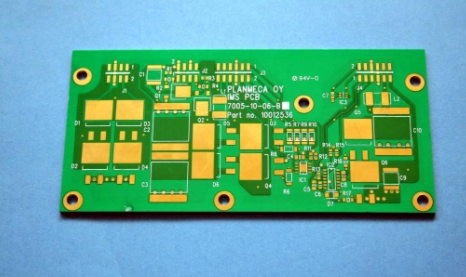
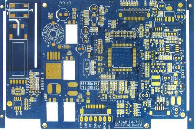
Small and medium batch circuit board manufacturers, focusing on high-precision PCB circuit boards, double-sided/multilayer circuit boards, HDI boards, blind buried via circuit boards, PCB high-frequency boards, special circuit boards, etc., (PCB, circuit boards, circuit boards), PCB proofing, circuit board proofing, circuit board manufacturers, Shenzhen circuit board factories, circuit board manufacturers, circuit board batch factories, PCB multilayer boards, circuit board manufacturers) for medical/security/industrial control/automotive/communication/military Years of production experience.