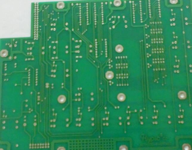
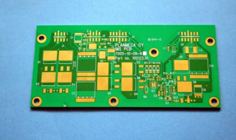
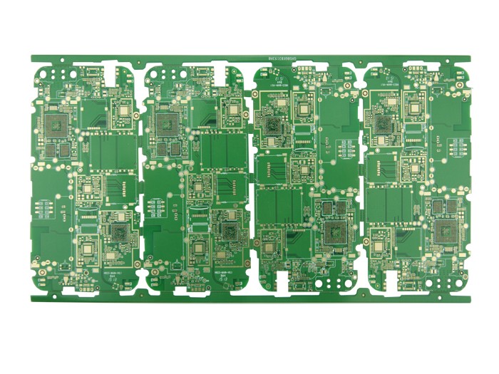
Definition and description of each layer of PCB multilayer circuit board
1. TOP LAYER (top layer wiring layer): Designed as the top copper foil wiring. If it is a PCB single-sided circuit board, there is no such layer.
2. BOMTTOM LAYER (bottom wiring layer): Designed as bottom copper foil routing.
3. TOP/BOTTOM SOLDER (top/bottom solder resist green oil layer): The top/bottom solder resist green oil is applied to prevent tin on the copper foil and maintain insulation. Open the window with solder mask at the pads, vias and non-electrical traces on this layer.
In the design, the pad will be opened by default (OVERRIDE: 0.1016mm), that is, the pad exposes the copper foil and expands by 0.1016mm, and it will be tinned during wave soldering. It is recommended not to make design changes to ensure solderability;
In the design of the via hole, the window will be opened by default (OVERRIDE: 0.1016mm), that is, the via hole exposes the copper foil, expands by 0.1016mm, and will be tinned during wave soldering. If the design is to prevent tin on the vias and not expose the copper, you must check the PENTING option in the additional properties of the vias SOLDER MASK (solder mask opening) to close the via opening.
In addition, this layer can also be used for non-electrical wiring separately, and the solder mask green oil will open the window accordingly. If it is on a copper foil trace, it is used to enhance the overcurrent capability of the trace, and tin is added during soldering; if it is on a non-copper foil trace, it is generally designed for logo and special character silk screen printing, which can save production Character silk screen layer.
4. TOP/BOTTOM PASTE (top/bottom solder paste layer): This layer is generally used to apply solder paste during the SMT reflow soldering process of SMT components, and has nothing to do with PCB circuit board manufacturers. It can be deleted when exporting GERBER. PCB Keep the default when designing the multilayer circuit board.

5. TOP/BOTTOM OVERLAY (top/bottom screen printing layer): Designed for various screen printing logos, such as component tag numbers, characters, trademarks, etc.
6. MECHANICAL LAYERS (mechanical layer): Designed as the mechanical shape of the PCB multilayer board, the default LAYER1 is the shape layer. Other LAYER2/3/4, etc. can be used for mechanical dimensioning or special purposes. For example, when certain PCB boardsneed to be made of conductive carbon oil, LAYER2/3/4, etc. can be used, but the purpose of the layer must be clearly marked on the same layer.
7. KEEPOUT LAYER (forbidden wiring layer): Designed as a forbidden wiring layer, many designers also use the mechanical shape of the PCB multilayer circuit board. If the PCB multilayer board has both KEEPOUT and MECHANICAL LAYER1, it mainly depends on the two layers. The shape integrity is generally subject to MECHANICAL LAYER1. It is recommended to use MECHANICAL LAYER1 as the shape layer when designing. If you use KEEPOUT LAYER as the shape, do not use MECHANICAL LAYER1 to avoid confusion!
8.MIDLAYERS (middle signal layer): mostly used for multilayer circuit boards, our company's design is rarely used. It can also be used as a special-purpose layer, but the purpose of the layer must be clearly marked on the same layer.
9. INTERNAL PLANES (internal electrical layer): used for multi-layer circuit boards, our company design does not use.
10. MULTI LAYER (through hole layer): through hole pad layer.
11. DRILL GUIDE (drilling positioning layer): the center positioning coordinate layer of the pad and the hole drilling.
12.DRILL DRAWING (drilling description layer): the description layer of the hole diameter of the pad and the hole.
In DESIGN–OPTION:
(Signal layer), Internal Planes
(Internal power supply/ground plane), Mechanical
Layers (mechanical layers),
Masks (solder mask),
Silk screen (silk screen layer),
Others (other working level)
And System (system working layer),
Execute the menu command [Design]/[Options…] during PCB multi-layer board design to set the visibility of each working layer.
One, Signal Layers (signal layer)
Protel98 and Protel99 provide 16 signal layers: Top (top), Bottom (bottom) and Mid1-Mid14 (14 middle layers).
The signal layer is the wiring layer used to complete the copper foil traces of the printed circuit board. When designing double panels, generally only two layers of Top (top layer) and Bottom (bottom layer) are used.
When the number of printed circuit boards exceeds 4 layers, Mid (middle wiring layer) is required.
Two, Internal Planes (internal power supply / ground plane)
Protel98 and Protel99 provide Plane1-Plane4 (4 internal power/ground planes). The internal power/ground layer is mainly used for (multilayer PCB) printed circuit boards with more than 4 layers as a dedicated wiring layer for power and grounding. Double-sided PCB boards do not need to be used.
Three, Mechanical Layers (mechanical layer)
The mechanical layer is generally used to draw the border (boundary) of the printed circuit board, usually only one mechanical layer is used. There are Mech1-Mech4 (4 mechanical layers).
Four, Drkll Layers (drilling position layer)
There are 2 layers: "Drill Drawing" and "Drill Guide". Used to draw the hole diameter and positioning of the hole.
Five, Solder Mask (solder mask)
There are 2 layers: Top (top) and Bottom (bottom). The solder mask is drawn on the protective area around the pads and vias on the printed circuit board.
Six, Paste Mask (Solder Paste Protective Layer)
There are 2 layers: Top (top) and Bottom (bottom). The solder paste protective layer is mainly used for printed circuit boards with surface-mounted components. At this time, it is required for the installation process of surface-mounted components, and this layer is not required when there are no surface-mounted components.
Seven, Silkscreen (silk screen layer)
There are 2 layers: Top (top) and Bottom (bottom). The silk screen layer is mainly used to draw text descriptions and graphic descriptions, such as the contours, labels and parameters of components.
Eight, Other (other layers)
There are 8 layers: "Keep Out", "Multi Layer", "Connect", "DRC Error", 2 "Visible Grid" Layers)” “Pad Holes (pad hole layer)” and “Via Holes (via hole layer)”. Some of these layers are used by the system itself, such as the Visible Grid (visible grid layer) for the designer to facilitate positioning when drawing. And Keep Put (no wiring layer) is used for automatic wiring, manual wiring is not required.
For hand-drawn double-sided printed circuit boards, the most used are Top Layers (top copper foil wiring), Bottom Layers (bottom copper foil wiring) and Top Silkscreen (top silk screen layer). You can choose a color you are used to for each layer, generally red for the top layer, blue for the bottom layer, green or white for text and symbols, and yellow for pads and vias.