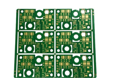
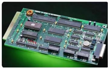
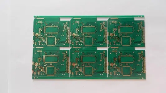
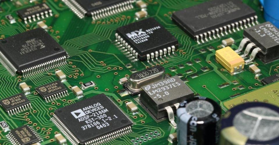
Printed circuit board is referred to as PCB. PCB is mainly composed of insulating substrate and conductor. It is the provider of electronic components connection. It plays the role of support and interconnection in electronic equipment. It is the organic combination of electronic, mechanical, chemical materials and other electronic equipment products. In short, PCB is the lifeblood of every electronic product.
5G RF PCB market is big
In 2019, the output value of PCBs in the world is 54.2 billion US dollars, and the growth rate of the industry in the past five years has not exceeded 3%. Countries and regions that compete in the PCB industry include the United States, Europe, Japan, Chinese mainland, Taiwan, Korea and so on. In 2016, the output value of PCBs in Chinese mainland amounted to 27 billion 100 million US dollars, accounting for 50% of the world total. The market predicts that China will be the region with the fastest growth in PCBs production in the next five years. By 2020, the market size will reach 35.9 billion US dollars, with an annual compound growth rate of about 3.1%.

Printed circuit board
PCB industry upstream is copper plate, downstream covers all circuit products. PCB demand for communication equipment, computers and consumer electronics accounted for 28. 8%, 265% and 14%. They account for 3% and nearly 70% of the total demand respectively, which are the three regions with the highest demand for PCBs. It is estimated that in the four years from 2017 to 2021, communication (communication equipment) and automotive electronics will become the new driving force to promote the development of PCBs industry, with a compound annual growth rate of 7% and 6% respectively. The application of communication network construction in PCB is mainly in wireless network, transmission network, data communication and fixed network broadband. In the early stage of 5g construction, the increasing demand for PCB is reflected in the wireless network and transmission network, and the demand for PCB backplane, high-frequency board and high-speed multi-layer board is large.
The value of base station PCB will increase greatly
The application of massivemimo in 5g era has brought great changes to base station structure. Antenna + RRU + BBU has become AAU + BBU (Cu / DU) architecture. In AAU, the antenna oscillator and micro transceiver unit array are directly connected to the Printed circuit board, which integrates digital signal processing module (DSP), digital to analog converter (DAC) / analog to digital converter (ADC), amplifier (PA), low noise amplifier (LNA), filter and other devices as RRU functions.
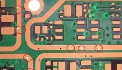
The requirements of antenna integration are significantly improved. AAU needs to integrate more components in smaller size and use more layer PCB technology. Therefore, the PCB consumption of a single base station will increase significantly. Its process and raw materials need to be upgraded comprehensively, and the technical barriers will be upgraded comprehensively. "The transmission power of 5g base station is far greater than 4G, which requires PCB to upgrade its substrate comprehensively, such as high frequency, high speed, good heat dissipation performance, small and stable dielectric constant and medium loss, consistent with the thermal expansion coefficient of copper foil as far as possible, low water absorption, other heat resistance, chemical resistance, impact strength, peeling strength, etc. PCB processing difficulty will also be greatly improved, high-frequency high-speed logistics, chemical performance and general Printed circuit board.
Different, lead to different processing technology, the same PCB needs to achieve a variety of functions, different materials mixed, therefore, the value of PCB will be further improved.
The volume and quantity of BBU have little change, but due to the increase of transmission rate and the decrease of transmission delay, the requirement of BBU for RF information processing ability is improved, and the demand for high-speed PCB is greatly increased. The core configuration of BBU is a backboard and two boards (main control board and baseband board). The backplane is mainly used to connect single boards and realize signal transmission. It has the characteristics of high multi-layer, super large size, ultra-high thickness, super heavy weight and high stability. This is a very difficult problem to deal with. It is the PCB with the highest unit price in the base station. The single board is responsible for RF signal processing and RRU connection, mainly using high-speed multi-layer PCB. With the increase of high-speed data exchange scenarios in 5g era, the number and consumption of high-speed material backplane and single board will further increase. The number of layers on the back and on the veneer will increase from 18 to 20 to 30. Copper laminates need to be upgraded from traditional FR4 materials to high-speed materials with better performance, such as M4 / 6 / 7, thus increasing the price per square meter.
Market space calculation of base station Printed circuit board
According to market data, 4G data circuit and RF account for about 60% of RRU area, and PCB area for 4G base station data circuit and RF is about 0.2m2. However, with the increase of data transmission and processing by base station AAU in 5g era, the area of data circuit and RF PCB is expected to double, that is, about 0.4m2. Since the base station feed network and antenna oscillator are integrated on the PCB, the area of the feed network and antenna oscillator is approximately equal to the area of the main board. According to Huawei's data, the area and height of the main station of 64r64r base station are 0.6m and 0.4m respectively, so the area of antenna oscillator + feed network is about 0.5m2, and the PCB area of 5g base station AAU is about 0.9m2, which is 4.5 times of the area of PCB in 4G era.
In addition, the number of oscillators in the antenna array is more, and the arrangement is closer. Therefore, the baseboard of the antenna array needs high-quality PCB. By optimizing the radiation unit and array mode, the mutual impedance can be reduced and the overall efficiency can be improved. With the increase of massivemimo channels, the area and number of layers per PCB will also increase from 15 to 35 square centimeters. The number of layers is upgraded from double-sided board to about 12 layers, and the substrate needs high-speed and high-frequency materials. According to market data, the unit price of 5 GPCB is about 2000 yuan per square meter. Assuming that each base station has three antennas, the Printed circuit board cost of a single base station is estimated to be about 6000 yuan. Assuming that the unit price of large-scale production decreases by 5% year by year, it is estimated that the PCB market space required for the construction of base stations will be about 29% by 2026. 2 billion yuan. If the number of 5g base stations in the world is taken into account, the demand for Du, Cu and backplane and the construction of small base stations will be even greater.