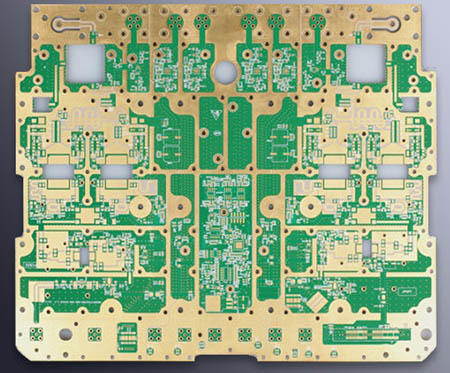
Circuit board manufacturing process
now formally cut into the process of manufacturing circuit boards. Some people will say, don’t you explain the circuit board design, why do you spend so much effort to introduce the circuit board craftsmanship?
This is because whether it is circuit design or circuit board design, it is for the subsequent production of good circuit boards to realize the value of its development and the purpose of mass production. If we regard production failure as a good opponent, then we should get to know our opponent well. Know yourself and the enemy. Let's take a look at Yuwei Electronics and everyone about the manufacturing process of the circuit board.
The manufacturing process of the circuit board
1. Use Laserphotoplotters to draw the film to make wiring film, solder mask film, printing film and other necessary films in the manufacturing process. During the film pasting process, there will be some errors, especially for special plate making, the error will be larger. Therefore, the influence of these errors should be fully considered in the circuit board design, and a suitable design should be made.

2. Cutting of the board. The size of the board for manufacturing the circuit board when it leaves the factory is usually 1m*1m or 1m*1.2m. According to the production needs, cut into different sizes of work pieces (work), according to the size of the circuit board designed by oneself to choose the established work piece size, to avoid waste and increase unnecessary costs.
3. Formation of the inner layer circuit Next, the inner layer circuit wiring is formed (1-5 in Fig. 2). Paste the photosensitive dry film (dryfilm) on the double-sided copper plate as the inner layer, and then stick the film used to make the inner layer wiring, expose it, and then perform the development process, leaving only the wiring required The place. This project must be carried out on both sides, through the etching ((Etching)) device to remove the unnecessary copper foil. Figure 8 1~5.
4. Oxidation treatment (blackening treatment) Before being combined with the outer layer, the copper foil should be oxidized to form a fine uneven surface. This is to increase the contact area between the insulating and adhesive prepreg and the inner layer to make the adhesion better. Nowadays, in order to reduce environmental pollution, alternatives to oxidation treatment have been developed, and today's circuit boards themselves have good contact.
5. After the lamination process of the multi-layer PCB is laminated as shown in Figure 8, the inner layer circuit after the oxidation process is covered with a semi-curing agent, and then the outer layer copper plate is pasted. In a vacuum state, it is heated and compressed by a laminator. The semi-curing agent plays the role of adhesion and insulation. After lamination, the appearance of the double-sided copper board looks the same, and the subsequent engineering is the same as that of the double-sided copper board.
6. Hole-opening CNC machine tools perform hole-opening operations.
7, PCB multi-layer board removal residues will melt due to the heat generated during the opening of the hole, and will adhere to the inner wall of the electroplated hole, which can be removed by chemicals to smooth the inner wall and increase the reliability of copper plating.
8. Copper plating: The inner and outer layer connections need to be processed by copper plating. First, electroless plating is used to form the minimum thickness that can flow current. Secondly, in order to achieve the plating thickness required by the design, electrolytic plating is performed. Because the outer copper foil is also coated with copper, the thickness of the outer trace is the thickness of the copper foil plus the thickness of the electroplating.
9. The formation of the outer layer circuit is the same as that of the inner layer circuit. Paste a photosensitive dry film, and then close the wiring film on the surface to expose. After the exposure, only the places needed for wiring are left, double-sided All are processed, and then the unnecessary copper foil is removed by etching.
10. The solder resist layer of the circuit board is made to form the pad, and the solder resist layer (insulation layer) needs to be formed, and it is also to protect the copper foil and better insulation. The method can be by directly pasting the film, or first coating the resin and then pasting the film, and removing unnecessary areas through exposure and development.
11. The surface treatment of the circuit board has no solder resist and exposed copper parts. In order to prevent oxidation, lead, lead-free copper plating, electrolytic or electroless gold plating, or water-soluble chemical cleaning agents are required for surface treatment.
12. Printing and printing are usually white, and the solder mask is green. For the LED light circuit board, in order to achieve a better effect of strengthening the light source, the printing is black and the solder mask is white. Or simply dispense with printing.
Printing can play a great auxiliary meaning for installing and checking the number of electronic components. But in order to keep the circuit confidential, sometimes the printing is sacrificed.
13. Shape processing The circuit board shape is processed by CNC punching machine tool or mold
14. The electrical testing project uses special electrical testing equipment to detect the open circuit and short circuit of the circuit board
15. Shipment: After checking the appearance and quantity of the circuit board, it can be shipped. Usually, it is packaged with deoxidized materials or directly taken to the factory where the components are installed.