Circuit board manufacturers: why do circuit boards need test points
Test points for circuit board manufacturers: For those who learn electronic circuits, it is natural to set up test points on the circuit boards, but for those who learn machinery, what are the test points?
Basically, the purpose of setting test points is to test whether the components on the circuit board meet the specifications and solderability. For example, if you want to check whether there is any problem with the resistance on a circuit board, the easiest way is to measure with a multimeter. You can know it by measuring both ends.
However, there is no way for you to use an electric meter to slowly measure every resistance, capacitance, inductance, and even the circuit of the IC on each board in a large-volume circuit board production factory, so there is the so-called The emergence of the ICT (In-Circuit-Test) automated test machine, which uses multiple probes (generally called "Bed-Of-Nails" fixtures) to simultaneously contact all the needs on the boards of the circuit board manufacturers The circuit of the parts to be measured is then programmed to measure the characteristics of these electronic parts in a sequence-based, parallel-assisted manner. Generally, testing all parts of a general circuit board takes only 1 to 2 minutes to complete., Depending on the number of parts on the circuit board, the more parts the longer the time.

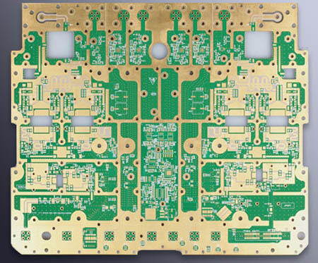
But if these probes directly touch the electronic parts on the board of the circuit board manufacturer or its solder feet, it is very likely that some electronic parts will be crushed, and it will be counterproductive. So smart engineers invented "test points". A pair of small round dots are additionally led out at both ends of the part, and there is no mask on the top, so that the test probe can contact these small points without directly contacting the electronic parts to be measured.
In the early days when there were traditional plug-in (DIP) on the circuit board, the solder feet of the parts were indeed used as test points, because the solder feet of the traditional parts were strong enough to not be afraid of needle sticks, but there were often probes. The misjudgment of poor contact occurs, because after general electronic parts are subjected to wavesoldering or SMT tin, a residual film of solder paste flux is usually formed on the surface of the solder. The impedance of this film is very high. High, often cause poor contact of the probe, so test operators on the production line were often seen at that time, often holding an air spray gun to blow desperately, or use alcohol to wipe these places that need to be tested.
In fact, the test points after wave soldering will also have the problem of poor probe contact. Later, after the popularity of SMT, the misjudgment of the test was greatly improved, and the application of test points was also given a great deal of responsibility, because the parts of SMT are usually very fragile and cannot withstand the direct contact pressure of the test probe. Use test points. This eliminates the need for the probe to directly contact the parts and their solder feet, which not only protects the parts from damage, but also indirectly greatly improves the reliability of the test, because there are fewer misjudgments.
However, with the evolution of technology, the size of the circuit board has become smaller and smaller. It is already a bit difficult to squeeze so many electronic parts on the small circuit board. Therefore, the problem of the test point occupying the circuit board space is often There is a tug-of-war between the design side and the manufacturing side, but this topic will be discussed later when there is a chance. The appearance of the test point is usually round, because the probe is also round, which is easier to produce, and it is easier to bring the adjacent probes closer, so that the needle density of the needle bed can be increased.
1. Using a needle bed for circuit testing has some inherent limitations on the mechanism, for example: the minimum diameter of the probe has a certain limit, and the needle with too small diameter is easy to break and damage.
2. The distance between the needles is also limited, because each needle must come out of a hole, and the back end of each needle must be welded with a flat cable. If the adjacent holes are too small, except for the needle and the needle. There will be a contact short-circuit problem, and the interference of the flat cable is also a big problem.
3. Needles cannot be implanted beside some high parts. If the probe is too close to the high part, there is a risk of collision with the high part and cause damage. In addition, because of the high part, it is usually necessary to make holes in the needle bed of the test fixture to avoid it, which indirectly makes it impossible to implant the needle. Test points for all parts that are increasingly difficult to accommodate on the circuit board.
4. As the PCB boards of circuit board manufacturers are getting smaller and smaller, the storage and waste of test points have been repeatedly discussed. Now there are some methods to reduce test points, such as Nettest, TestJet, BoundaryScan, JTAG, etc.; there are others as well. The test method of the company wants to replace the original needle bed test, such as AOI and X-Ray, but it seems that each test cannot replace ICT 100%.
Regarding the ability of ICT to implant needles, you should ask the matching PCB manufacturer, that is, the minimum diameter of the test point and the minimum distance between adjacent test points. There is usually a desired minimum value and a minimum value that the ability can achieve. Large-scale circuit board manufacturers will require that the distance between the minimum test point and the minimum test point cannot exceed a few points, otherwise the jig will be easily damaged.