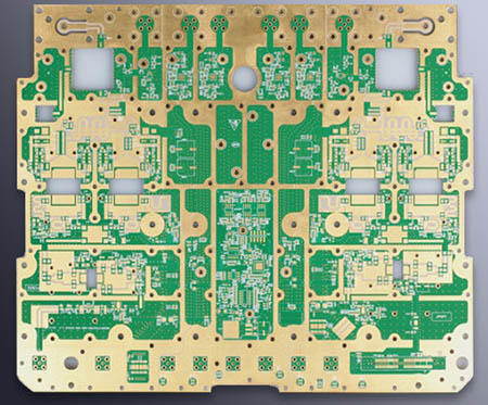
Printed circuit board appearance inspection machine is an important quality inspection equipment in PCB production line. Based on the principle of optical image processing and computer vision identification technology, its main function is to detect the appearance defects encountered in the production process of PCB components. China is the world's PCB production country, but it is not power, an important link of PCB production chain, PCB equipment instrument is not strong is one of the important reasons of the state, to promote the development and progress of China PCB industry, has developed the automatic inspection machine operation is simple, the system is more compact and higher price performance ratio of the PCB appearance inspection machine manually.

1. Overall structure of PCB appearance checker system
PCB on-line inspection system has a complex structure, and its transmission control equipment, electrical control system and camera must be under the control of the computer to coordinate the processing work and complete the complex inspection and sorting tasks. The structure of PCB online inspection equipment based on machine vision.
Analysis of basic structure and working principle of PCB on-line testing equipment
FIG. 1 Structure of PCB online inspection equipment based on machine vision
The system is mainly divided into motion control, image acquisition and image processing. Image acquisition is an important part of the whole system. The camera and lens are the equivalent of the human eye in machine vision and are responsible for taking the image of the subject. Image acquisition is an important part of PCB detection system and the basis of detection and processing. PCB detection system emphasizes detection speed and accuracy, so it needs the image acquisition part to provide clear images timely and accurately.
2. Hardware structure of image acquisition system
1) Working principle of image acquisition system
When the system is powered on, MCU automatically detects whether the PCB platform is reset to the starting point. This process is mainly accomplished by two optical fiber sensors and servo motors. Two sensors are installed at the starting point of the sigu motor track, namely the reset point and the end point of the track. Reset, stop and motor reversal function. When MCU detects that THE SESorL (reset point or starting point) is invalid after power-on, the motor reversal program is called to make the PCB platform return to the starting point, and the serial port sends invalid color picture signal to PC. Then MCU continues to judge whether there is a button pressed. If there is a button pressed, the motor starts to turn forward, and the serial port sends a valid color picture signal to the PC. This process is PCB line scanning process to complete the image collection. This process motor goes through three stages: acceleration stage, uniform color graph stage and deceleration stop stage. In the process of motor forward rotation, starting from 7 o 'clock, MCU counts the pulses fed back by the servo motor encoder through the special capture comparison unit (CCU6), but when the count value reaches the effective value of drawing, the serial port sends the starting signal of drawing to PC, and then the linear CCD starts to collect the PCB image. When the motor decelerates and turns to senor2, the sensor at the end of the track, the motor stops and immediately reverses back to the starting point. In this process, the serial port sends an invalid signal for drawing to the PC. So far a complete detection process is complete. MCU continues to detect whether there is a button pressed down for detection. The effective signal and start signal sent by serial port can avoid triggering by mistake. The image signal collec
ted by CCD is sent to the image acquisition card by CamreLink interface for further image processing by PC.
Analysis of basic structure and working principle of PCB on-line testing equipment
2) Receiving and detection of sensors and buttons
Using optocoupler isolation technology, can achieve photoelectric isolation between circuits, even if the input signal can pass unimpeded, and prevent the output signal feedback to the input end, favorable suppression of peak pulse and various noise interference, stable work, no contact, long service life, high transmission efficiency. In order to detect the feedback rotation speed signal of the rotary mirror in real time, high-speed photocoupler ACPL-072L is adopted in this design. The transmission rate can be as high as 25 MBd.
Analysis of basic structure and working principle of PCB on-line testing equipment
In this design, the capture/comparison unit CC25 port is used in XC164CS peripherals, and the photocoupler transmission signal is used as external interrupt signal to trigger XC164, so as to realize high-speed sensing positioning and button detection.
3) CCD camera system
The image acquisition system of the manual PCB appearance checker adopts NUCLi7300, a 3CCD color line scanning camera of NED Rainbow series. The camera has a wide range of applications and can detect color differences that were previously impossible with black and white cameras. The external interface is a high-speed serial interface (Camera Link), which can be conveniently connected with the acquisition card, conveniently set the gain and offset, and has the function of correcting the RGB line delay. The pixel number is 7 300x3 Line, the pixel size is 10x10 μm, the data rate is 60MHz, and the short scan rate is 7.6khz. Figure 4 is the sequential diagram of the continuous line scan rate model used in this system.
Analysis of basic structure and working principle of PCB on-line testing equipment
The image acquisition card in the system adopts SoliosXCL-SU74 from Matrox Company. The card has its own processor to process two independent base mode or one medium mode Camera Link configuration, 66 MHz acquisition rate, 64 MB buffer, and can collect surface array and line array cameras, and has a variety of acquisition modes.
Currently, most image detection systems on the market use Areascan cameras to collect and analyze images. However, due to the large size range of PCB products inspected by this PCB appearance inspection machine -- 50 mmx50mm ~ 330mmx250 mm, the accuracy is required to reach sub-pixel level. The resolution and image acquisition speed of plane scanning camera can not meet these requirements, so the system chooses line scanning CCD. However, the detection system of line scan must use the speed of movement to obtain the area image, that is, when the PCB being measured moves to the camera field of view, the hardware sends trigger signal to the camera to start acquisition, so the acquisition mode of the acquisition card is set to hardware trigger synchronous acquisition, and 64 M memory is allocated. The connection diagram of CCD and acquisition card is shown in Figure