What are the difficulties in making multi-layer circuit boards
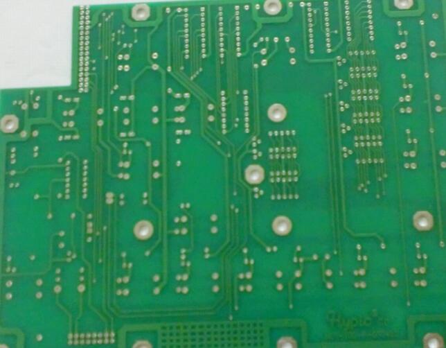
In the circuit board industry, multi-layer circuit boards (high-precision PCB multi-layer boards) are generally defined as 4 layers-20 layers or more called multi-layer circuit boards, which are more difficult to process than traditional PCB multi-layer circuit boards, and their quality is reliable. High performance requirements, mainly used in communication equipment, industrial control, security, high-end servers, medical electronics, aviation, military and other fields. In recent years, the market demand for high-level PCB boards in applications such as communications, base stations, aviation, and military has remained strong. With the rapid development of China's telecommunications equipment market, the market prospects for high-level PCB boards have been promising.
At present, domestic high-level circuit board manufacturers that can mass produce circuit boards are mainly foreign-funded enterprises or a few domestic-funded enterprises. The production of high-level circuit boards not only requires high technology and equipment investment, but also requires the accumulation of experience of technicians and production personnel. At the same time, the import of PCB multi-layer circuit boards has strict and cumbersome customer certification procedures. Therefore, the threshold for high-level circuit boards to enter the enterprise is relatively high. The realization of industrialized production cycle is longer.
The average number of layers of PCB multi-layer boards has become an important technical indicator to measure the technical level and product structure of PCB companies. This article briefly describes the main processing difficulties encountered in the production of high-level circuit boards, and introduces the control points of the key production processes of high-level circuit boards for your reference.
1. Difficulties in making main circuit boards
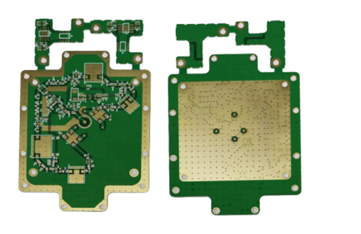
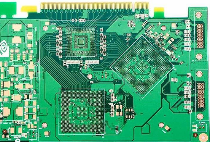
Compared with the characteristics of conventional circuit boards, high-level circuit boards have the characteristics of thicker PCB boards, more layers, denser lines and vias, larger unit sizes, thinner dielectric layers, etc., inner layer space and interlayer alignment., Impedance control and reliability requirements are more stringent.
1. Difficulties in alignment between layers
Due to the large number of high-level PCB layers, the customer design side has more and more stringent requirements for the alignment of each layer of the PCB. Usually, the alignment tolerance between layers is controlled at ±75μm. Considering the high-level board unit size design and the ambient temperature and humidity of the graphics transfer workshop, And factors such as misalignment and superposition caused by inconsistency of expansion and contraction of different core layers, interlayer positioning methods, etc., make it more difficult to control the alignment of high-rise boards.

2. Difficulties in the production of the inner line
PCB high-level circuit boards use special materials such as high TG, high speed, high frequency, thick copper, thin dielectric layer, etc., which puts forward high requirements for the production of inner circuit and pattern size control, such as the integrity of impedance signal transmission, which increases the production of inner circuit Difficulty. Small line width and line spacing, more open and short circuits, more short circuits, and low pass rate; more fine line signal layers, the probability of missing AOI detection in the inner layer is increased; the inner core plate is thinner, which is easy to wrinkle and cause poor exposure and etching It is easy to roll the board when passing the machine. Most of the multi-layer circuit boards are system boards, and the unit size is relatively large. The cost of scrapping the finished product is relatively high.
3. Difficulties in pressing and making
Multiple PCB inner core boards and prepregs are superimposed, and it is easy to produce defects such as slippage, delamination, resin voids and air bubbles during production. When designing a laminated structure, it is necessary to fully consider the heat resistance of the material, withstand voltage, the amount of glue and the thickness of the medium, and set a reasonable PCB high-level circuit board pressing program. There are many layers, the expansion and contraction amount control and the size coefficient compensation amount cannot be kept consistent, and the interlayer insulation layer is thin, which easily leads to the failure of interlayer reliability testing. Figure 1 is a defect diagram of the delamination of the plate after the thermal stress test.
4. Difficulties in drilling drilling
Using high-TG, high-speed, high-frequency, thick copper special plates, increasing the difficulty of drilling roughness, drilling burrs and de-drilling. There are many layers, the cumulative total copper thickness and the plate thickness, the drilling is easy to break the knife; the dense BGA is many, the CAF failure problem caused by the narrow hole wall spacing; the plate thickness is easy to cause the inclined drilling problem.
2. Key production process control
1, PCB material selection
With the development of high-performance and multi-functional electronic components, high-frequency, high-speed development of signal transmission is brought about, so the dielectric constant and dielectric loss of electronic circuit materials are required to be relatively low, as well as low CTE and low water absorption. Rate and better high-performance copper clad laminate materials to meet the processing and reliability requirements of high-level boards. Commonly used board suppliers mainly include A series, B series, C series, and D series. The main characteristics of these four inner substrates are compared, see Table 1. For high-rise thick copper circuit boards, use prepregs with high resin content. The amount of glue flowing between the interlayer prepregs is sufficient to fill the inner layer pattern. If the insulating dielectric layer is too thick, the finished board may be too thick. On the contrary, if the insulating dielectric layer is too thin, it is easy to cause Quality issues such as dielectric delamination and high-voltage test failure, so the selection of insulating dielectric materials is extremely important.
2, laminated laminated structure design
The main factors considered in the design of the laminated structure are the heat resistance of the material, the withstand voltage, the amount of filler, and the thickness of the dielectric layer. The following main principles should be followed.
1. . When customers require high TG sheets, the core board and prepreg must use the corresponding high TG materials.
2. . The prepreg and core board manufacturers must be consistent. In order to ensure PCB reliability, avoid using a single 1080 or 106 prepreg for all layers of prepreg (except for special requirements of customers). When the customer has no media thickness requirements, the thickness of the interlayer media must be guaranteed ≥0.09mm in accordance with IPC-A-600G.
3. . For the inner substrate 3OZ or above, use prepregs with high resin content, such as 1080R/C65%, 1080HR/C68%, 106R/C73%, 106HR/C76%; but try to avoid the structural design of 106 high-adhesive prepregs. In order to prevent multiple 106 prepregs from superimposing, because the glass fiber yarn is too thin, the glass fiber yarn collapses in the large substrate area, which affects the dimensional stability and the delamination of the plate.
4. . If the customer has no special requirements, the thickness tolerance of the interlayer dielectric layer is generally controlled by +/-10%. For the impedance board, the dielectric thickness tolerance is controlled by IPC-4101C/M tolerance. If the impedance influencing factor is related to the thickness of the substrate, The sheet tolerance must also be in accordance with IPC-4101C/M tolerance.
3, interlayer alignment control
The accuracy of the inner core board size compensation and the production size control requires the data and historical data collected in the production for a certain period of time to accurately compensate the size of each layer of the multilayer circuit board to ensure that each layer of the core board Consistency of expansion and contraction. Choose a high-precision, high-reliability interlayer positioning method before pressing, such as four-slot positioning (PinLAM), hot melt and rivet combination. Setting the appropriate pressing process and routine maintenance of the press is the key to ensuring the quality of the pressing, controlling the glue flow and cooling effect of the pressing, and reducing the problem of interlayer misalignment. The layer-to-layer alignment control needs to comprehensively consider factors such as the inner layer compensation value, the pressing positioning method, the pressing process parameters, and the material characteristics.
4. Inner circuit technology
Since the resolution capability of the traditional exposure machine is about 50μm, for the production of high-level boards, a laser direct imaging machine (LDI) can be introduced to improve the resolution of graphics, and the resolution can reach about 20μm. The alignment accuracy of the traditional exposure machine is ±25μm, and the alignment accuracy between layers is greater than 50μm. Using a high-precision alignment exposure machine, the graphic alignment accuracy can be increased to about 15μm, and the interlayer alignment accuracy can be controlled within 30μm, which reduces the alignment deviation of traditional equipment and improves the interlayer alignment accuracy of the high-level board.
In order to improve the etching ability of the circuit, it is necessary to give proper compensation to the width of the circuit and the pad (or solder ring) in the engineering design, but also to make a more detailed design for the compensation amount of the special pattern, such as the return circuit and the independent circuit. consider. Confirm whether the design compensation of inner line width, line distance, isolation ring size, independent line, and hole-to-line distance is reasonable, otherwise change the engineering design. There are impedance and inductive reactance design requirements. Pay attention to whether the design compensation of independent line and impedance line is sufficient, control the parameters during etching, and mass production can be done after the first piece is confirmed to be qualified. In order to reduce the etching side corrosion, it is necessary to control the composition of each group of the etching solution within the optimal range. The traditional etching line equipment has insufficient etching capability, and it is possible to carry out technical transformation of the equipment or introduce high-precision etching line equipment to improve etching uniformity and reduce etching burrs and unclean etching.
5, pressing process
The current positioning methods between layers before pressing mainly include: four-slot positioning (PinLAM), hot melt, rivet, hot melt and rivet combination, and different product structures adopt different positioning methods. For multilayer circuit boards, the four-slot positioning method (PinLAM), or the fusion + riveting method is used, the positioning hole is punched out by the OPE punching machine, and the punching accuracy is controlled within ±25μm. When fusing, adjust the machine to make the first board to use X-RAY to check the layer deviation, and the layer deviation can be produced in batches. During mass production, it is necessary to check whether each plate is fused into the unit to prevent subsequent delamination. The pressing equipment adopts high-performance supporting equipment. The press meets the alignment accuracy and reliability of the high-level board.
According to the laminated structure of the multilayer circuit board and the materials used, study the appropriate pressing procedure and set the best heating rate and curve. In the conventional multilayer circuit board pressing procedure, appropriately reduce the heating rate of the laminated sheet. Extend the high-temperature curing time to make the resin flow and cure fully, and at the same time avoid the problems of sliding plate and interlayer dislocation during the pressing process. Plates with different material TG values cannot be the same as grate plates; plates with common parameters cannot be mixed with plates with special parameters; to ensure the rationality of the expansion and shrinkage coefficients given, the properties of different plates and prepregs are different, and the corresponding plates must be used The prepreg parameters are pressed together, and the special materials that have never been used need to verify the process parameters.