Teach you to understand the process flow of PCB multilayer circuit boards
Double-sided circuit board is the middle layer of medium, and both sides are wiring layers. The PCB multi-layer circuit board is a multi-layer wiring layer, and there is a dielectric layer between every two layers, and the dielectric layer can be made very thin. Multilayer circuit boards have at least three conductive layers, two of which are on the outer surface, and the remaining layer is integrated into the insulating board. The electrical connection between them is usually achieved through plated through holes on the cross section of the circuit board.
High assembly density, small size, and light weight. Due to the high assembly density, the wiring between components (including components) is reduced, thereby improving reliability; the number of wiring layers can be increased, thereby increasing design flexibility; A circuit with a certain impedance; it can form a high-speed transmission circuit; it can be equipped with a circuit, magnetic circuit shielding layer, and a metal core heat dissipation layer to meet the needs of special functions such as shielding and heat dissipation; simple installation and high reliability.
The cost is high; the cycle is long; high-reliability testing methods are required. Multilayer printed circuit is the product of the development of electronic technology in the direction of high speed, multi-function, large capacity and small volume. With the continuous development of electronic technology, especially the extensive and in-depth application of large-scale and very large-scale integrated circuits, multilayer printed circuits are rapidly developing in the direction of high density, high precision, and high-level digitalization. Fine lines and small apertures have appeared., Blind and buried holes, high plate thickness to aperture ratio and other technologies to meet the needs of the market.

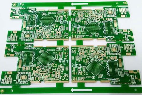
Multi-layer PCB circuit board is a kind of printed circuit board which is laminated and bonded by alternating conductive pattern layers and insulating materials. The number of layers of the conductive pattern is more than three, and the electrical interconnection between the layers is realized through metallized holes. If one double-sided circuit board is used as the inner layer, two single-sided boards are used as the outer layer, or two double-sided boards are used as the inner layer and two single-sided boards are used as the outer layer, the positioning system and the insulating bonding material are laminated together, and the conductive The graphics are interconnected according to the design requirements and become four-layer, six-layer, and eight-layer circuit boards, also known as multi-layer PCB circuit boards.
Compared with the production process of general PCB multi-layer boards and double-sided circuit boards, the main difference is that PCB multi-layer boards have added several unique process steps: inner layer imaging and blackening, lamination, etchback and de-drilling. In most of the same processes, certain process parameters, equipment accuracy and complexity are also different. For example, the inner metallization connection of the multi-layer board is the decisive factor for the reliability of the multi-layer board, and the quality requirements for the hole wall are stricter than that of the double-layer board, so the requirements for drilling are higher. In addition, the number of stacks for each drilling of the multi-layer board, the speed and feed rate of the drill bit during drilling are different from those of the double-sided board. The inspection of finished and semi-finished multi-layer boards is also much stricter and more complicated than double-sided boards. Due to the complex structure of the multi-layer board, a glycerin hot-melt process with uniform temperature should be used instead of an infrared hot-melt process that may cause excessive local temperature rise.
1. Remove oil, impurities and other pollutants on the surface;
2. The oxidized surface is not affected by moisture at high temperatures, reducing the chance of delamination between the copper foil and the resin.
3. Make the non-polar copper surface into a surface with polar CuO and Cu2O, and increase the polar bond between the copper foil and the resin;
4. Increase the specific surface of the copper foil, thereby increasing the contact area with the resin, which is conducive to the full diffusion of the resin and the formation of greater bonding force;
5. The board with the inner circuit must be blackened or browned before it can be laminated. It is to oxidize the copper surface of the inner board. Generally, the produced Cu2O is red and CuO is black, so the Cu2O-based oxide layer is called browning, and the CuO-based oxide layer is called blackening.
1. Laminating is the process of bonding each layer of circuits into a whole by means of a B-stage prepreg. This bonding is achieved through mutual diffusion and penetration between macromolecules at the interface, and then interweaving. The process of bonding the various layers of circuits into a whole by the stage prepreg. This bonding is achieved through mutual diffusion and penetration between macromolecules at the interface, and then interweaving.
2. Purpose: to press discrete PCB multi-layer boards and adhesive sheets together to form PCB multi-layer boards with the required number of layers and thickness.
1. The laminated circuit board is sent to the vacuum heat press during the lamination process. The heat energy provided by the machine is used to melt the resin in the resin sheet, thereby bonding the substrate and filling the gap.
2. Lamination For designers, the first thing that needs to be considered for lamination is symmetry. Because the board will be affected by pressure and temperature during the lamination process, there will still be stress in the board after the lamination is completed. Therefore, if the two sides of the laminated board are not uniform, the stress on the two sides will be different, causing the board to bend to one side, which greatly affects the performance of the PCB.
3. The typesetting is to stack the copper foil, bonding sheet (prepreg), inner layer board, stainless steel, isolation board, kraft paper, outer layer steel plate and other materials according to the process requirements. If the board is more than six layers, pre-typesetting is required. Laminate copper foil, bonding sheet (prepreg), inner layer board, stainless steel, isolation board, kraft paper, outer layer steel plate and other materials according to the process requirements. If the board is more than six layers, pre-typesetting is required.
In addition, even in the same plane, if the distribution of copper is uneven, the resin flow speed at each point will be different, so that the thickness of the place with less copper will be slightly thinner, and the thickness of the place with more copper will be thicker. Some. In order to avoid these problems, various factors such as the uniformity of copper distribution, the symmetry of the stack, the design and layout of blind and buried vias, etc. must be carefully considered during the design.
Purpose: to metalize the through hole.
1. The substrate of the circuit board is composed of copper foil, glass fiber, and epoxy resin. In the production process, the hole wall section after the base material is drilled is composed of the above three parts of materials.
2. Hole metallization is to solve the problem of covering a uniform layer of copper with heat shock resistance on the cross section. Hole metallization is to solve the problem of covering a uniform layer of copper with heat shock resistance on the cross section.
3. The process is divided into three parts: one de-drilling process, two electroless copper process, and three thick copper process (full board copper electroplating).
The metallization of holes involves a concept of capacity, the ratio of thickness to diameter. The thickness-to-diameter ratio refers to the ratio of the plate thickness to the hole diameter., Thickness to diameter ratio. The thickness-to-diameter ratio refers to the ratio of the plate thickness to the hole diameter. When the board continues to thicken and the hole diameter continues to decrease, it becomes more and more difficult for the chemical solution to enter the depth of the hole. Although the electroplating equipment uses vibration, pressure and other methods to allow the solution to enter the center of the hole, the center is caused by the difference in concentration. It is still unavoidable that the coating is too thin. At this time, there will be a slight open circuit phenomenon in the drilling layer. When the voltage increases and the board is impacted under various severe conditions, the defects are completely exposed, causing the circuit of the board to be disconnected and unable to complete the specified work.
Therefore, designers need to understand the process capability of the board manufacturer in time, otherwise the designed PCB board will be difficult to realize in production. It should be noted that the thickness-to-diameter ratio parameter must be considered not only in the design of through holes, but also in the design of blind and buried holes.
The principle of outer layer pattern transfer is similar to that of inner layer pattern transfer, both using photosensitive dry film and photographing methods to print circuit patterns on the board. The difference between the outer dry film and the inner dry film is:
1. If the subtractive method is used, the outer dry film is the same as the inner dry film, and the negative film is used as the board. The cured dry film part of the board is the circuit. The uncured film is removed, and the film is retreated after acid etching, and the circuit pattern remains on the board because of the protection of the film.