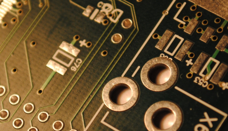
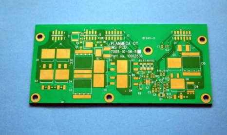
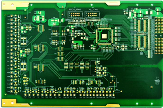
Talking about the production process of each layer of circuit board
This article mainly introduces: single-sided circuit board, double-sided circuit board sprayed tin plate, double-sided circuit board plated nickel gold, multilayer circuit board sprayed tin plate, multilayer circuit board nickel-plated gold, multilayer circuit board immersed nickel gold Board; The production process of each layer of circuit board is introduced in detail.
1. Single-sided circuit board process: blanking and edging - drilling - outer layer graphics - (full board gold plating) - etching - inspection - silk screen solder mask - (hot air leveling) - silk screen characters - shape processing - test - inspection.
2. The process flow of double-sided circuit board tin spraying board blanking and grinding - drilling - sinking copper thickening - outer layer graphics - tinning, etching tin removal - secondary drilling - inspection - silk screen solder mask - gold-plated plug - hot air Leveling-Silk-printed characters-Shape processing-Test-Inspection.
3. The process flow of nickel and gold plating on double-sided circuit boards is blanking and grinding - drilling - heavy copper thickening - outer layer graphics - nickel plating, gold removal and etching - secondary drilling - inspection - silk screen solder mask - silk screen characters - Shape processing-test-inspection.
4. Multi-layer circuit board tin spraying board process cutting edge grinding - drilling positioning hole - inner layer pattern - inner layer etching - inspection - blackening - lamination - drilling - heavy copper thickening - outer layer pattern - tinning, Etching tin removal-secondary drilling-inspection-screen printing solder mask-gold-plated plug-hot air leveling-screen printing characters-shape processing-test-inspection.

5. Multilayer circuit board nickel-gold plating process: blanking and edge grinding - drilling positioning holes - inner layer graphics - inner layer etching - inspection - blackening - lamination - drilling - sinking copper thickening - outer layer graphics - gold plating, Film removal and etching-secondary drilling-inspection-screen printing solder mask-screen printing characters-shape processing-test-inspection.
6. Multi-layer circuit board nickel-gold plate process: blanking and edge grinding - drilling positioning hole - inner layer pattern - inner layer etching - inspection - blackening - lamination - drilling - sinking copper thickening - outer layer pattern - plating Tin, etching tin removal-secondary drilling-inspection-screen printing solder mask-electroless nickel deposition-screen printing characters-shape processing-test-inspection.
iPCB is a high-tech manufacturing enterprise focusing on the development and production of high-precision PCBs. iPCB is happy to be your business partner. Our business goal is to become the most professional prototyping PCB manufacturer in the world. Mainly focus on microwave high frequency PCB, high frequency mixed pressure, ultra-high multi-layer IC testing, from 1+ to 6+ HDI, Anylayer HDI, IC Substrate, IC test board, rigid flexible PCB, ordinary multi-layer FR4 PCB, etc. Products are widely used in industry 4.0, communications, industrial control, digital, power, computers, automobiles, medical, aerospace, instrumentation, Internet of Things and other fields.